copper retention on pcb board A comprehensive guide to copper pcb boards
If you are looking for What is Copper Pour in PCB? - RayMing PCB you've came to the right web. We have 25 Pictures about What is Copper Pour in PCB? - RayMing PCB like Copper Recovery From PCB | PDF | Copper | Printed Circuit Board, copper pcb - H-CELERITY and also What is the role of copper laying in PCB design? Why should PCB lay. Read more:
What Is Copper Pour In PCB? - RayMing PCB
 www.raypcb.com
How To Extract Copper From Waste Pcb Board? – Nanjing Sure Origin
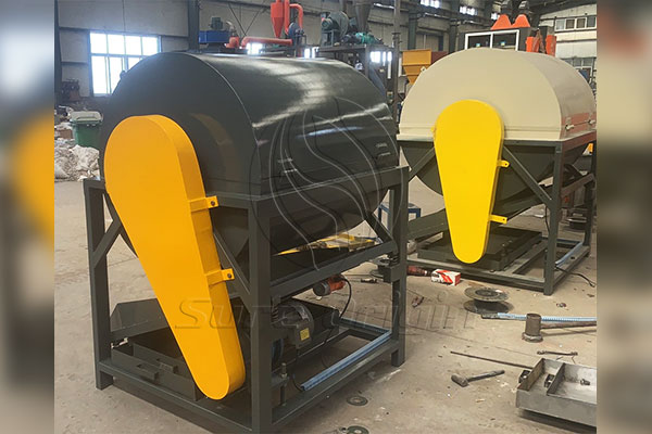 es.metalrecyclingplant.com
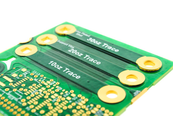
What Is The Weight Of Copper In Heavy Copper PCB Design?
 www.rocket-pcb.com
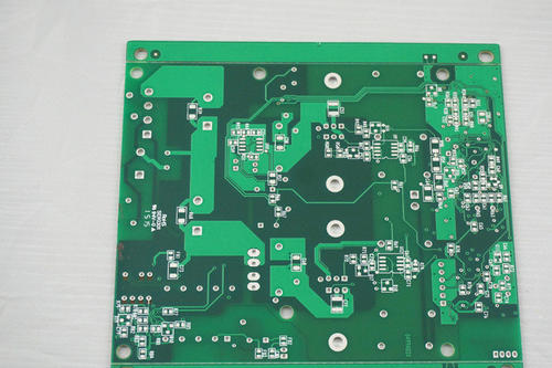
A Comprehensive Guide To Copper PCB Boards
 www.elepcb.com
PCB Copper Trace Width And Space: Everything You Need To Know About
 www.jarnistech.com
JHYPCB's PCB Copper Thickness Capabilities - JHYPCB
 www.pcbelec.com
Analysis Of Copper Laying In PCB - Industrial News - News - Zhejiang
 www.neodensmt.com
What Is The Role Of Copper Laying In PCB Design? Why Should PCB Lay
 arisentecpcb.com
Heavy Copper Pcb Withstand Demanding Environmental Conditions
 hilelectronic.com
PCB Copper Thickness: A Complete Guide
 www.elepcb.com
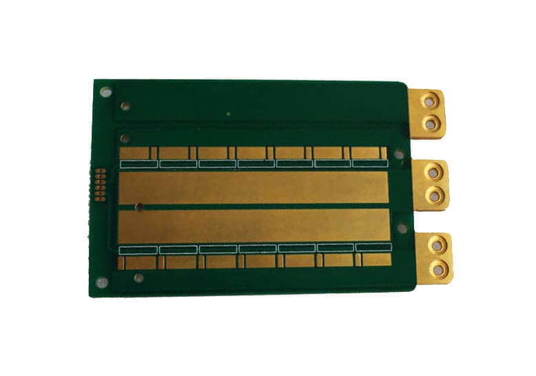
Heavy Copper PCB
 www.jycircuitboard.com
copper pcb
Copper Coined PCB
 home.fedevel.com
What Is PCB Copper Coating - A Complete Guide - IBE Electronics
 www.pcbaaa.com
Optimizing Your PCB: Copper Thickness For Peak Performance
 www.rowsum.com
Copper Pcb - H-CELERITY
 lightpcb.com
pcb copper
Heavy Copper And EXTREME Copper PCB Design For Maximum Reliability
 www.epectec.com
copper pcb heavy design 30oz features layer 20oz reliability extreme maximum 10oz 2oz featuring same sample figure
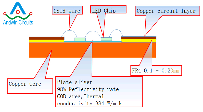
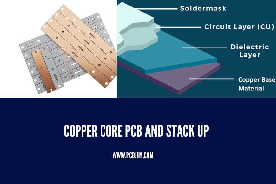
Copper Core PCB | Copper Base PCB Manufactruing - Andwin
 www.andwinpcb.com
copper pcb core direct path layer thermal cob dielectric substrate
Heavy Copper PCB – The Ultimate FAQs Guide - PCBA Manufacturers
 www.pcba-manufacturers.com
Pcb Copper Board - Copper Thickness | Electronics Forum (Circuits
PCB Circuit Board Copper Deposition Process Flow_Company News_News_KnownPCB
 www.knownpcb.com
Copper In Pcb - PCB Manufacturing And PCB Assembly Manufacturer
 www.andwinpcb.com
Copper Recovery From PCB | PDF | Copper | Printed Circuit Board
 www.scribd.com
PCB Copper Pour Basics
Copper Based PCB: Advanced Solutions & Manufacturing | JHYPCB
 www.pcbjhy.com
Heavy Copper PCB Applications - Canadian Circuits
 www.canadiancircuits.com
Copper pcb. What is the role of copper laying in pcb design? why should pcb lay. Copper in pcb