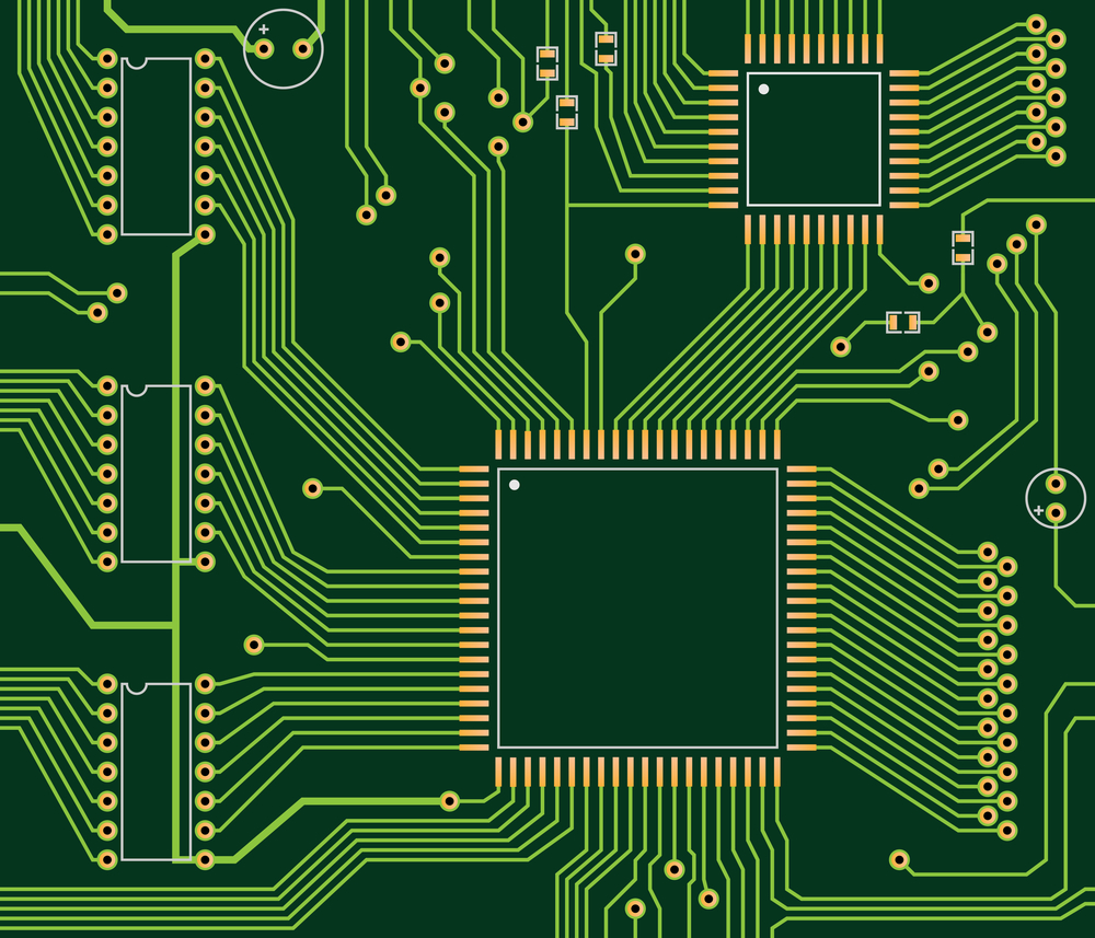
copper tracing on pcb board Pcb copper traces : kicad
If you are searching about PCB Copper Trace Width and Space: Everything You Need to Know About you've visit to the right place. We have 25 Pics about PCB Copper Trace Width and Space: Everything You Need to Know About like COPPER TRACE PCB Delhi, Maximizing Copper: Design Considerations for Printed Circuit Boards and also PCB Trace - Everything You Need To Know - AES. Read more:
PCB Copper Trace Width And Space: Everything You Need To Know About
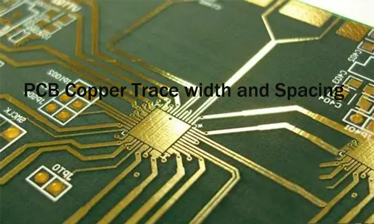 www.jarnistech.com
PCB Trace - Everything You Need To Know - AES
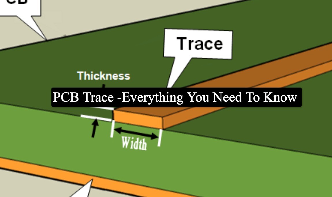 absolutepcbassembly.com
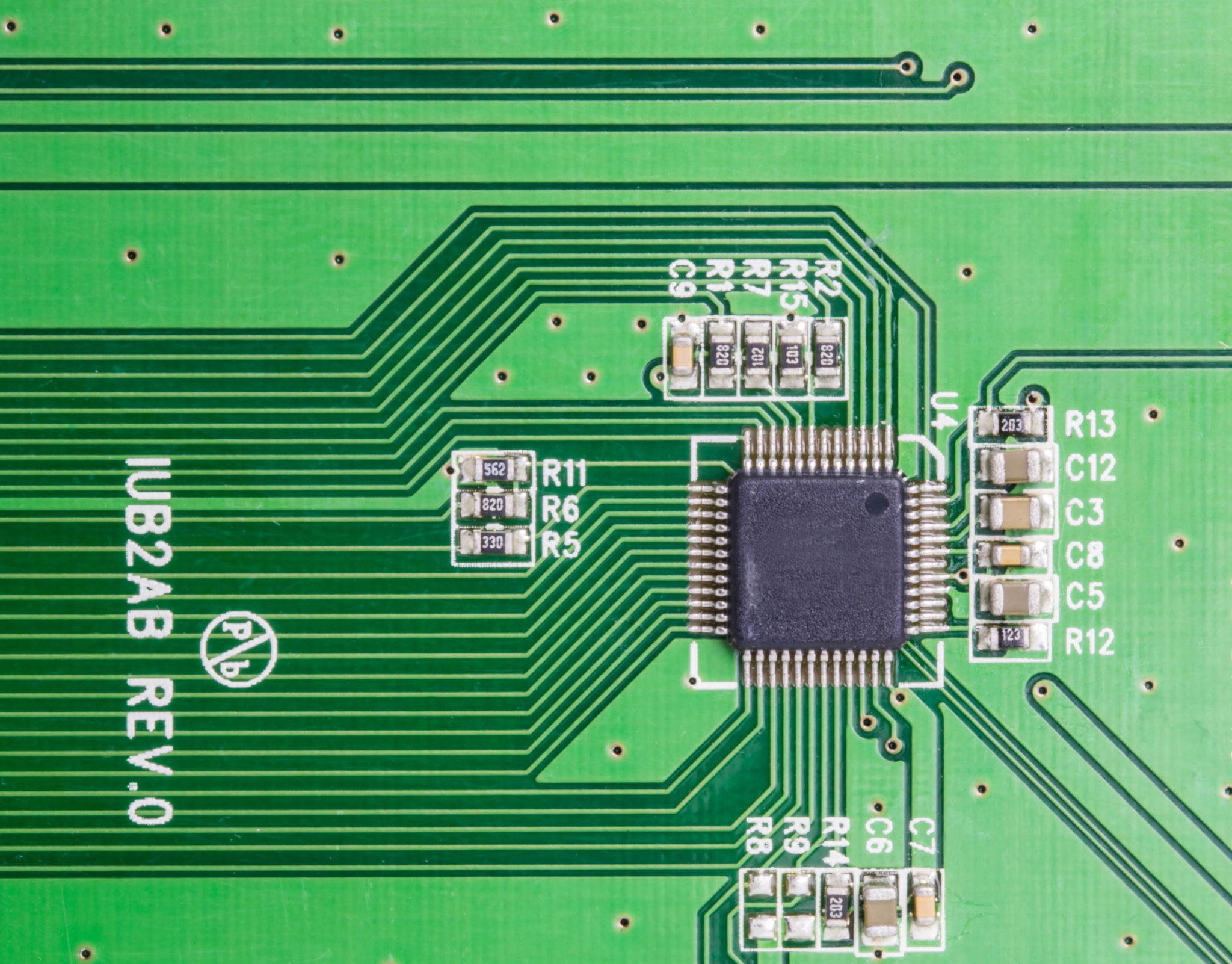
pcb trace
A Good Way To Apply Copper To PCB – PCB HERO
 www.pcb-hero.com
Determining Copper Trace Thickness In PCB Design
 www.linkedin.com
PCB Art, Design, Layout: Artfully Shaped Copper Traces - General - Lines
 llllllll.co
Why Do We Use Copper To Make PCB Traces? | Yun Industrial
 yic-assm.com
pcb traces yic assm
PCB Copper Thickness, Trace Width, And Current Relationship
 www.tf-pcb.com
Maximizing Copper: Design Considerations For Printed Circuit Boards
 www.scribd.com
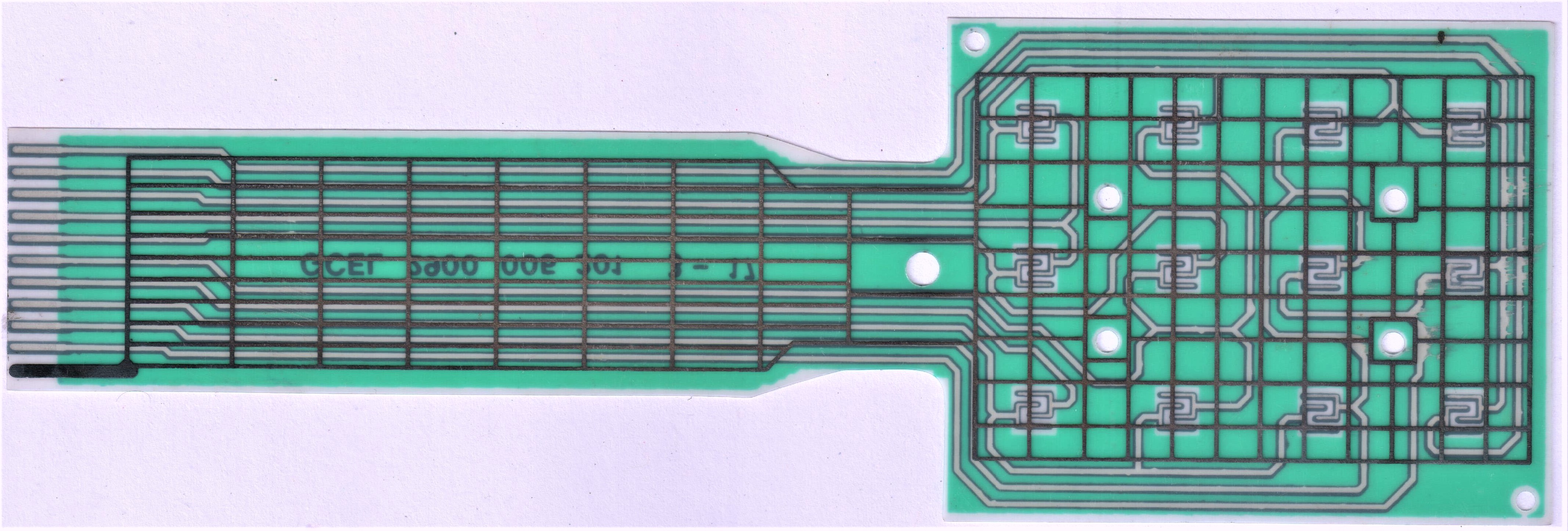
PCB Copper Traces : KiCad
 www.reddit.com
kicad traces copper pcb
A Brief Analysis On A PCB Copper Trace Capacity To Carry Current
 www.raypcb.com
pcb trace current thickness layer capacity electroplating brief power circuitry impedance desain tracing through 2221 ipc venture
PCB Copper Trace Width And Space: Everything You Need To Know About
 www.jarnistech.com
COPPER TRACE PCB Delhi
 coppertracepcb.in
What Are Copper Trace PCBs And Why Is It So Important?
 hilelectronic.com
QUESTION 1 [30 Marks] A Copper Track On A | Chegg.com
![QUESTION 1 [30 marks] A copper track on a | Chegg.com](https://media.cheggcdn.com/media/7c4/7c4b535c-1703-4d3f-8081-e26fee42554e/phpJELw5h.png) www.chegg.com
www.chegg.com
PCB Art, Design, Layout: Artfully Shaped Copper Traces In 2023 | Design
 www.pinterest.jp
Innovative Uses For Copper Traces In PCB Design
What Is A Copper Trace PCB And Why Is It Important? - RayMing PCB
 www.raypcb.com
Why Do We Use Copper To Make PCB Traces? | Yun Industrial
 yic-assm.com
pcb traces trace copper use circuit why printed make do boards we elan everything need know intl
3,059 Copper On Pcb Images, Stock Photos, 3D Objects, & Vectors
 www.shutterstock.com
Exposed Copper Tracing On PCB : Soldering
 www.reddit.com
PCB Art, Design, Layout: Artfully Shaped Copper Traces - General - Lines
 llllllll.co
USING HEAVY COPPER AND EXTREME COPPER IN PCB DESIGN AND FABRICATION FOR
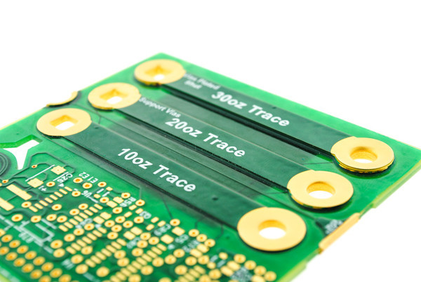 www.globalsmt.net
A Printed Circuit Board (PCB) Has Copper Wire Traces | Chegg.com
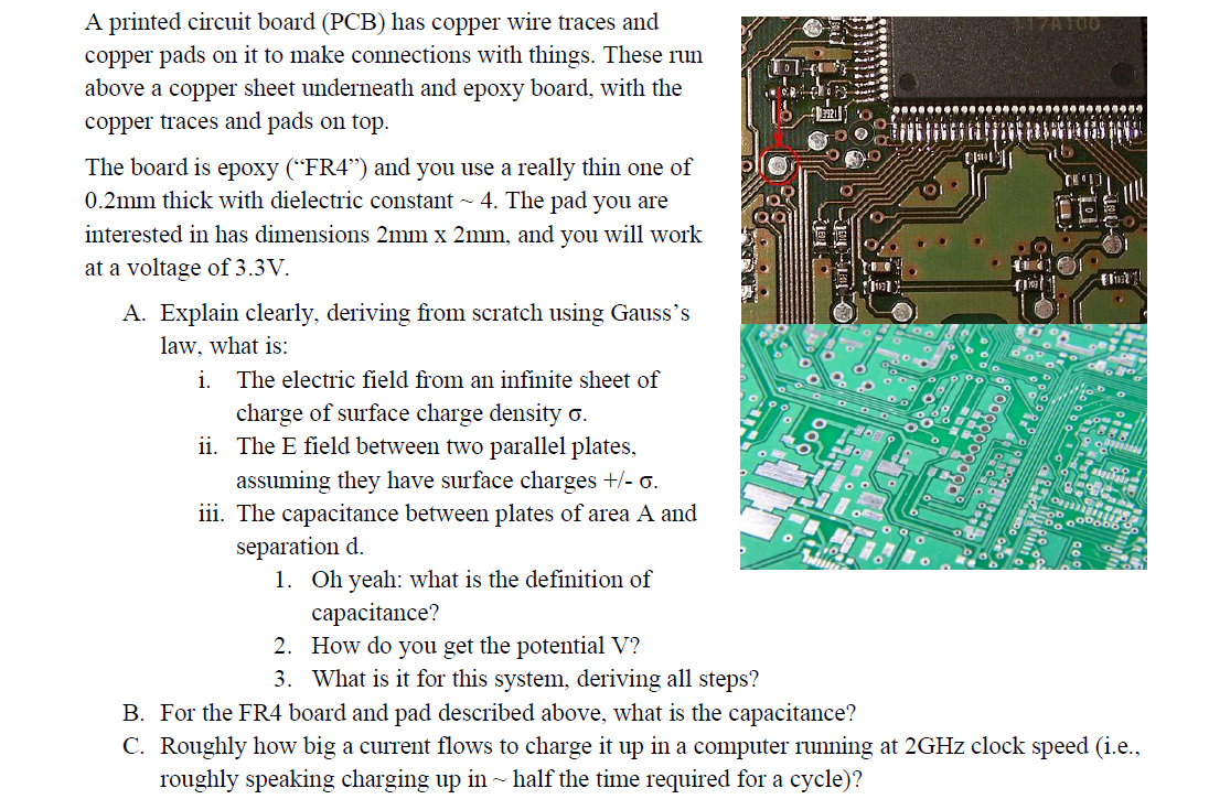 www.chegg.com
Innovative Uses For Copper Traces In PCB Design
What Is A Copper Trace PCB And Why Is It Important? - RayMing PCB
 www.raypcb.com
Pcb art, design, layout: artfully shaped copper traces. Why do we use copper to make pcb traces?. A good way to apply copper to pcb – pcb hero