diy double layer pcb Pcb diy multilayer circuits hasan saad syed months Pcb multilayer
If you are searching about What is double-layer PCB and how is it made - complete guide - IBE you've visit to the right page. We have 25 Images about What is double-layer PCB and how is it made - complete guide - IBE like multilayer pcb, Why Multilayer PCB is used so widely? and also How To Make A Multilayer PCB At Home - A Beginners Guide. Here it is:
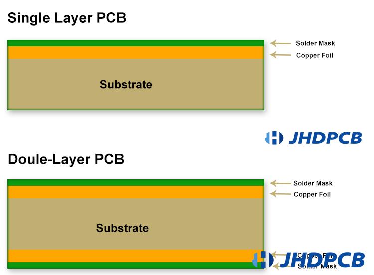
What Is Double-layer PCB And How Is It Made - Complete Guide - IBE
 www.pcbaaa.com
Multilayer Pcb Design [ From 2 Layers To 32 Lasers] - Design Your PCB Now
![Multilayer Pcb Design [ from 2 layers to 32 lasers] - Design Your PCB Now](https://www.venture-mfg.com/wp-content/uploads/2019/06/Figure-2-Double-layer-PCB.jpg) www.venture-mfg.com
www.venture-mfg.com
pcb layer double multilayer design
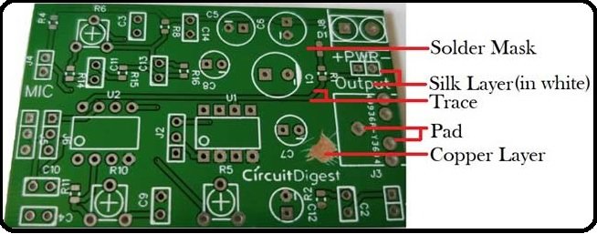
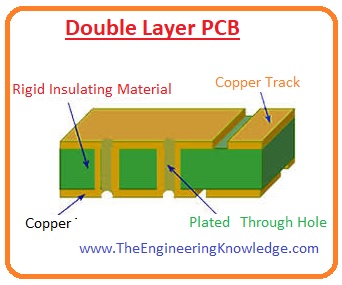
Introduction To Double Layer PCB - Construction And Working
 microcontrollerslab.com
pcb layer double construction introduction working
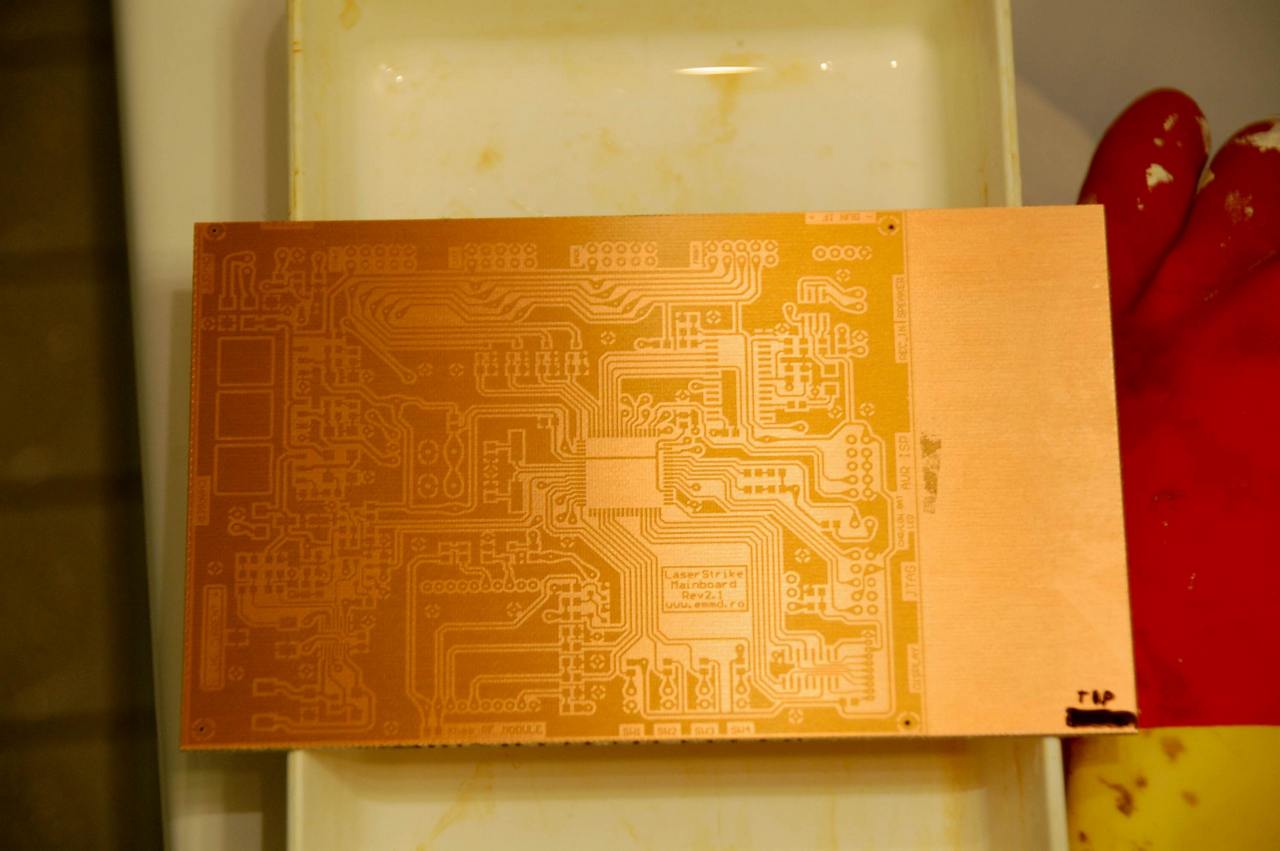
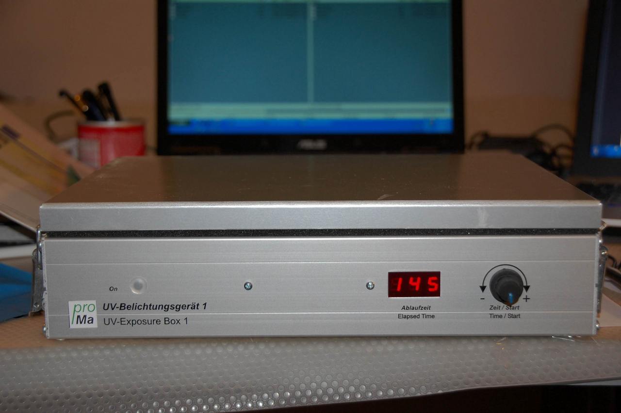
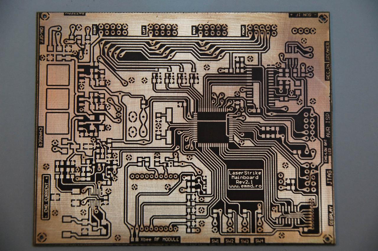
DIY: Double Sided PCB – Emmd Lab
 emmd.ro
DIY: Double Sided PCB – Emmd Lab
 emmd.ro
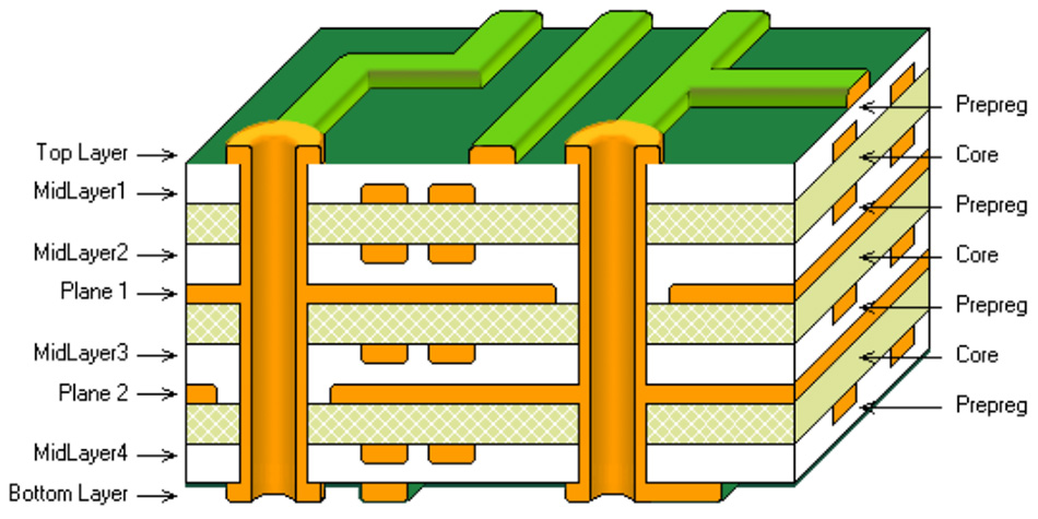
Multilayer PCB Design: An Introduction To The Basics
 pcbassemblymanufacturing.com
Introduction To Double Layer PCB - Construction And Working
 microcontrollerslab.com
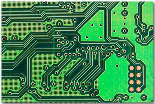
pcb
Multilayer PCB [Ultimate Guide] On Design And Manufacturing Process
![Multilayer PCB [Ultimate Guide] on Design and Manufacturing Process](https://www.circuitstoday.com/wp-content/uploads/2020/06/5_multilayer_pcb_process-450x316.png) www.circuitstoday.com
www.circuitstoday.com
pcb multilayer
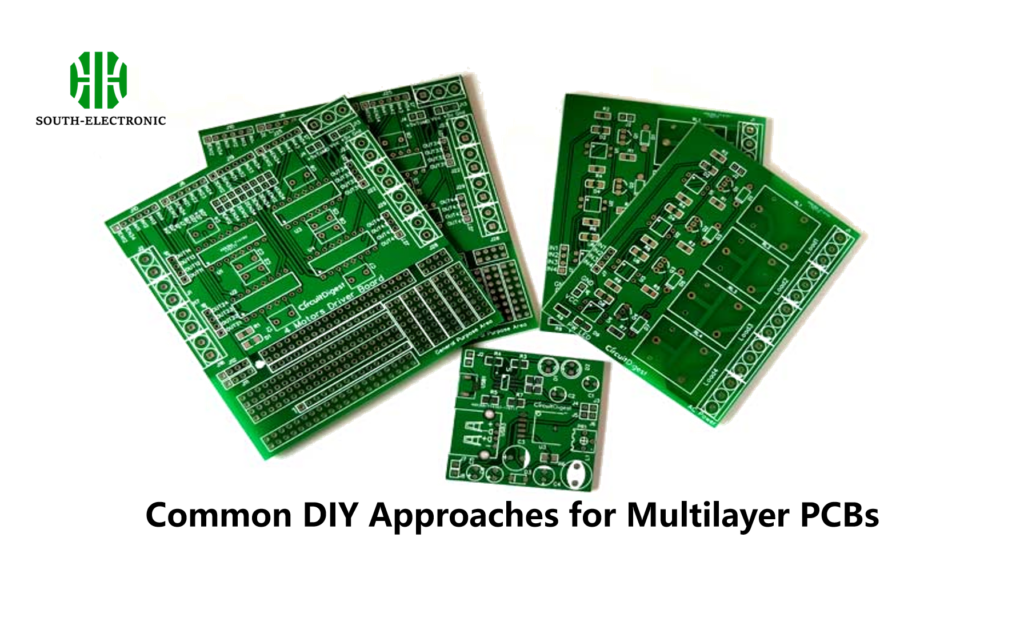
Common DIY Techniques For Multilayer PCB Fabrication
 southelectronicpcb.com
Pcb Mcrd V3 Double Layer What Is Multilayer Pcb? Definition
 pcbways.pages.dev
Multilayer PCB [Ultimate Guide] On Design And Manufacturing Process
![Multilayer PCB [Ultimate Guide] on Design and Manufacturing Process](https://www.circuitstoday.com/wp-content/uploads/2020/06/3_multilayer_pcb_design_process.png) www.circuitstoday.com
www.circuitstoday.com
pcb multilayer
PCB Multilayer Design Techniques And Their Applications - 86PCB
 86pcb.com
Introduction To Double Layer PCB The Engineering Projects, 53% OFF
 www.gf-planen.de
What Is Double Layer Pcb Introduction To Double Layer Pcb
 pcbways.pages.dev
How To Make A Multilayer PCB At Home - A Beginners Guide
 circuits-diy.com
pcb multilayer circuits
Everything You Should Know About Multilayer PCB - PCBA Manufacturers
 www.pcba-manufacturers.com
What Is Double-layer PCB And How Is It Made - Complete Guide - IBE
 www.pcbaaa.com
Multilayer Pcb
 www.circuits-diy.com
pcb multilayer circuits involved boards hasan syed saad
Why Multilayer PCB Is Used So Widely?
 circuits-diy.com
pcb multilayer widely routing pcbs circuits 1316
Diy Multilayer Pcb - PCB Manufacturing And PCB Assembly Manufacturer
 www.andwinpcb.com
What Is Double-layer PCB And How Is It Made - Complete Guide - IBE
 www.pcbaaa.com
How To Make A Multilayer PCB At Home - A Beginners Guide
 circuits-diy.com
pcb multilayer layer layers boards pcbs stackup prepreg tauschen akku gadgetronicx circuits conductive
Multilayer Pcb Design [ From 2 Layers To 32 Lasers] - Design Your PCB Now
![Multilayer Pcb Design [ from 2 layers to 32 lasers] - Design Your PCB Now](https://www.venture-mfg.com/wp-content/uploads/2019/06/Figure-3-Multi-layer-PCB.jpg) www.venture-mfg.com
www.venture-mfg.com
pcb multilayer layer multi circuit via vias what board printed boards pcbs design technology layers copper stackup traces layered through
Multilayer PCB Design: An Introduction To The Basics
 pcbassemblymanufacturing.com
DIY: Double Sided PCB – Emmd Lab
 emmd.ro
Pcb multilayer widely routing pcbs circuits 1316. Multilayer pcb design [ from 2 layers to 32 lasers]. Multilayer pcb design [ from 2 layers to 32 lasers]