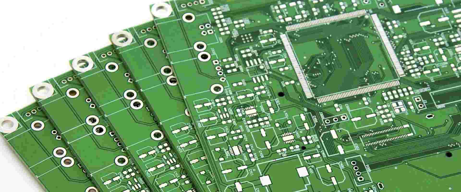
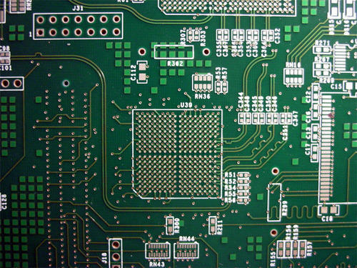
double layer pcb design pictures Pcb layer design board electronic practice
If you are searching about Double Layer PCB Design at Rs 60 in Coimbatore | ID: 17793398788 you've visit to the right web. We have 25 Pics about Double Layer PCB Design at Rs 60 in Coimbatore | ID: 17793398788 like Double Layer PCB Design - GGG CIRCUITS, Introduction to Double layer PCB - Construction and working and also Double Layer Pcb Design in Dadri | ID: 2851965413162. Read more:
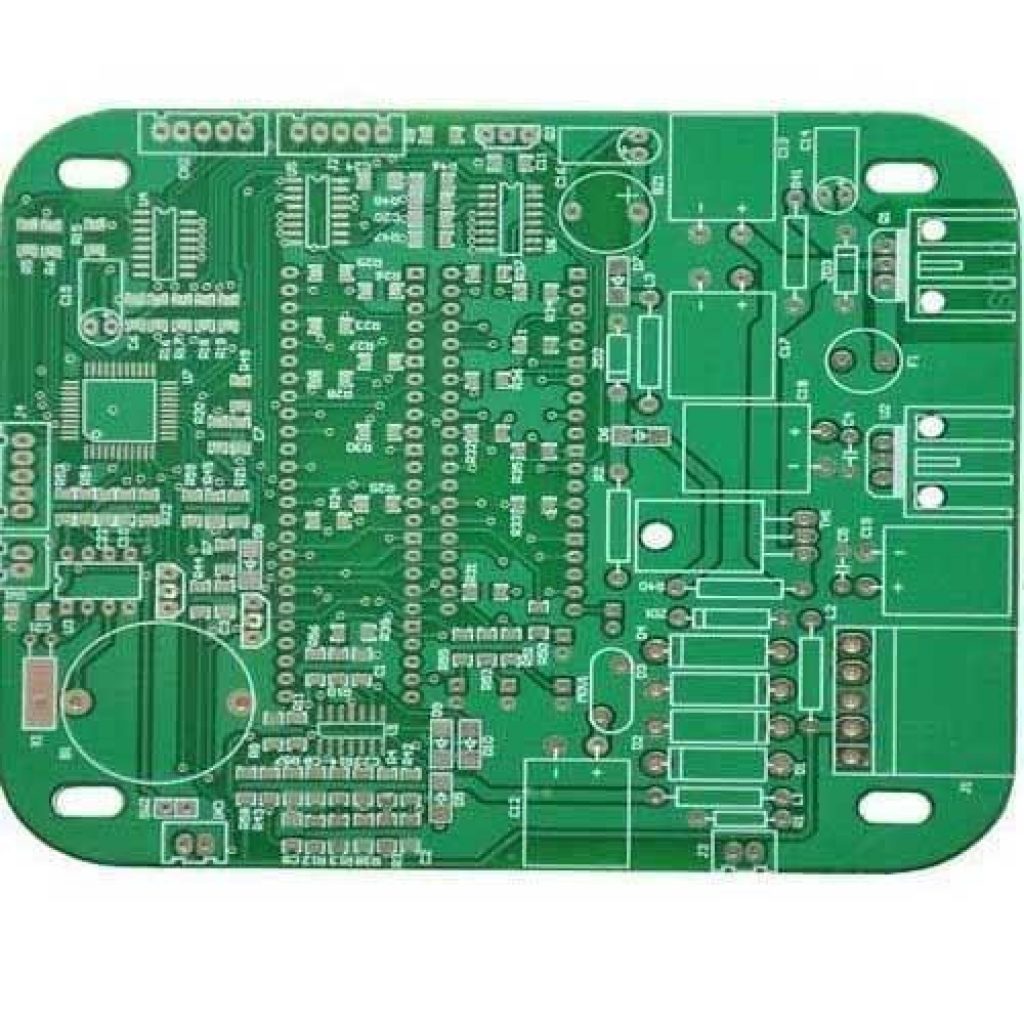
Double Layer PCB Design At Rs 60 In Coimbatore | ID: 17793398788
 www.indiamart.com
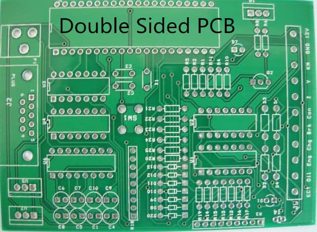
Double Layer PCB Design - GGG CIRCUITS
 www.gggcircuits.com
pcb cipsa
Double Layer Pcb Design In Dadri | ID: 2851965408633
 www.indiamart.com
Why Is 2 Layer PCB Popular In Electronic Industry ? – Swimbi
 swimbi.com
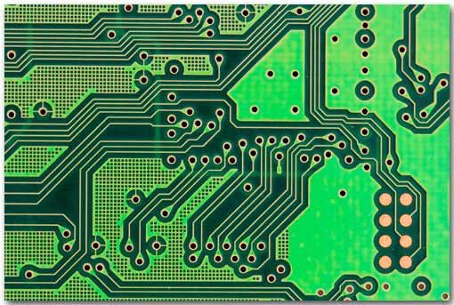
pcb double layer sided pcbs
Pcb Mcrd V3 Double Layer What Is Multilayer Pcb? Definition
 pcbways.pages.dev
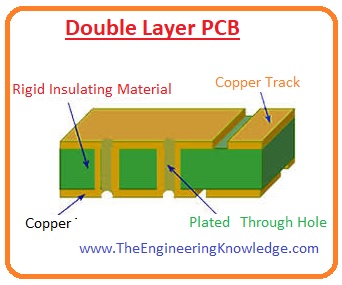
What Is Double-layer PCB And How Is It Made - Complete Guide - IBE
 www.pcbaaa.com
6 Layer Pcb Design Guidelines - Design Talk
 design.udlvirtual.edu.pe
Double Layer Pcb Design At Rs 16 In Dadri | ID: 2851965530348
 www.indiamart.com
What Is Double Layer Pcb Introduction To Double Layer Pcb
 pcbways.pages.dev
Double Layer PCB Design Service In Noida By Apeiron Innovations Private
 www.indiamart.com
Double Layer Pcb Design At Rs 16 In Dadri | ID: 2851965223373
 www.indiamart.com
What Is Double Layer Pcb Introduction To Double Layer Pcb
 pcbways.pages.dev
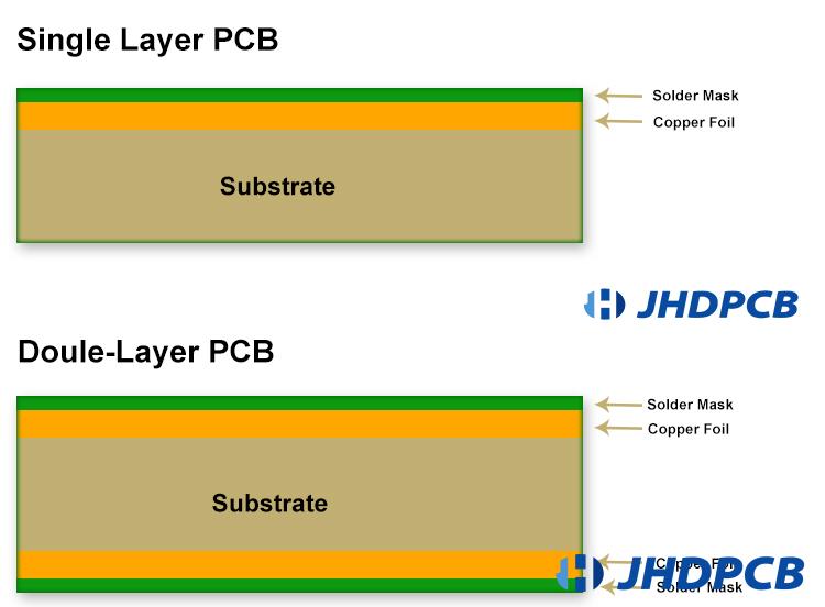
Introduction To Double Layer PCB The Engineering Projects, 53% OFF
 www.gf-planen.de
Pengertian Pcb Double Layer Pcb Layer Double Construction Applications
 pcbways.pages.dev
Double Layer Pcb Design In Dadri | ID: 2851965413162
 www.indiamart.com
2 Layer PCB Design Singapore | For Electronic Circuit
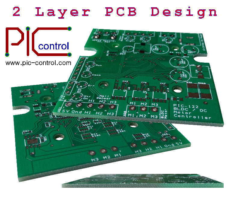 www.pic-control.com
pcb layer design board electronic practice
75 Components Double Layer PCB Design Service In New Delhi | ID
 www.indiamart.com
Double Layer PCB Design Service In New Delhi | ID: 22294353062
 www.indiamart.com
Double Layer Pcb Design In Dadri | ID: 2851965368148
 www.indiamart.com
Double Layer PCB Design At Rs 20 In Coimbatore | ID: 23279970862
 www.indiamart.com
Introduction To Double Layer PCB - Construction And Working
 microcontrollerslab.com
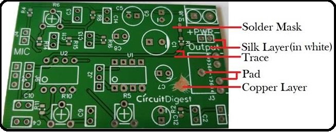
pcb
Double Layer PCB Designing In New Delhi | ID: 15557271630
 www.indiamart.com
Introduction To Double Layer PCB - Construction And Working
 microcontrollerslab.com
pcb layer double construction introduction working
Double Layer Pcb Design At Rs 16 In Dadri | ID: 2851965185255
 www.indiamart.com
Double Layer Pcb Design Service At Best Price In Vadodara | Dhruv
 www.tradeindia.com
What is double layer pcb introduction to double layer pcb. Pcb layer double construction introduction working. Double layer pcb design in dadri