high current pcb stack up Pcb stack-up guide & examples
If you are searching about PCB Layer Stackup, PCB Stackup Design | PCBCart you've visit to the right page. We have 25 Images about PCB Layer Stackup, PCB Stackup Design | PCBCart like pcb stack up impedance Multilayer pcb manufacturing cost, PCB stack-up – PCB HERO and also PCB Stackup Optimization: Engineering Robust Electronics. Here you go:
PCB Layer Stackup, PCB Stackup Design | PCBCart
 www.pcbcart.com
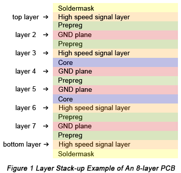
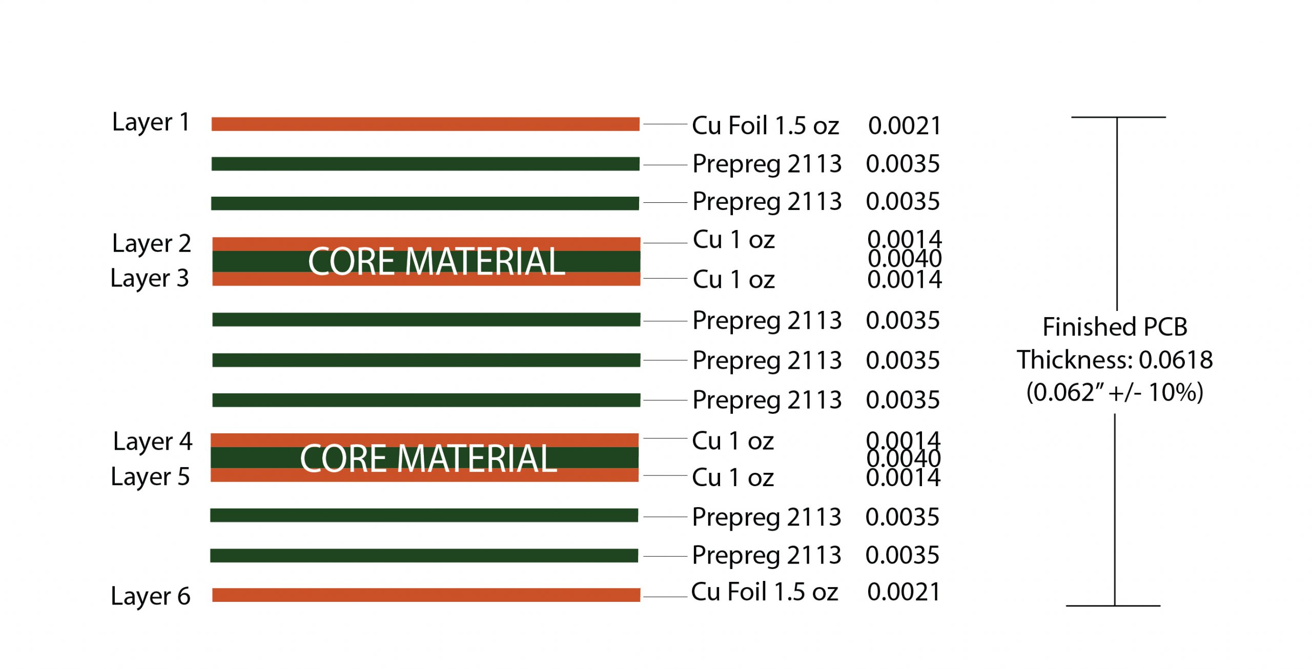
pcb layer stackup stack prepreg core layers multilayer example board what standard pool design circuit exactly power gnd plane signal
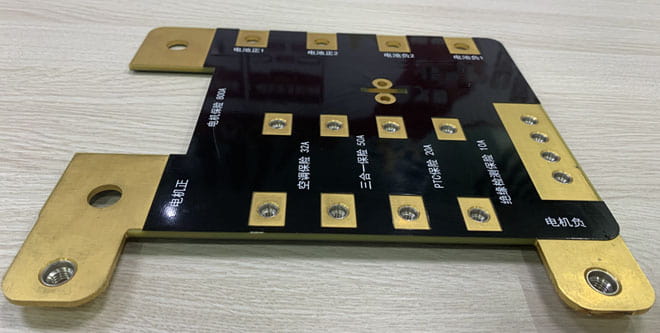
How To Design A High Current PCB - RAYPCB
 www.raypcb.com
pcb
PCB Stackup Design Principles - ABCPCB
 www.abcpcb.com
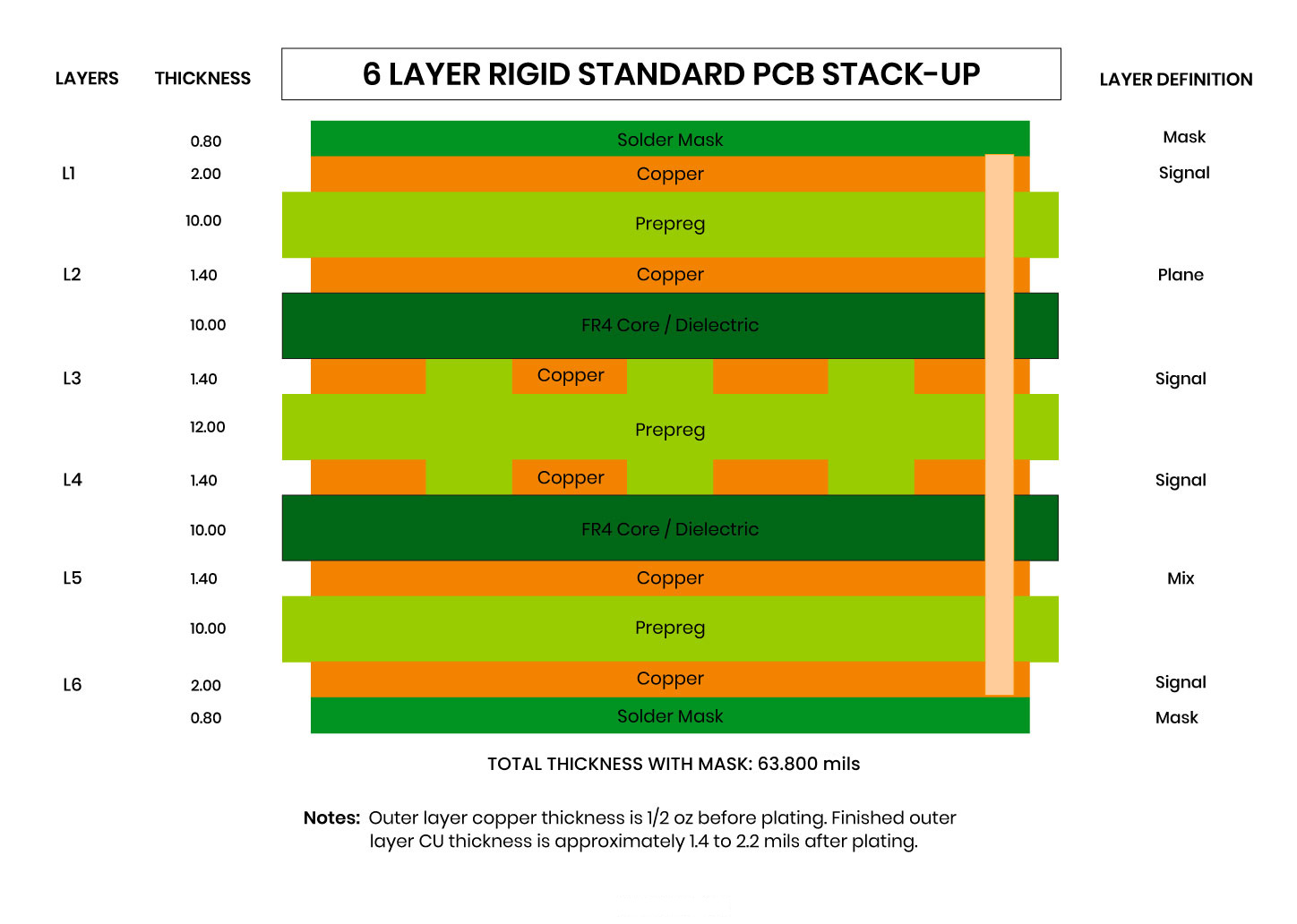
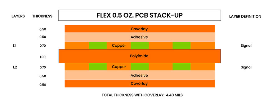
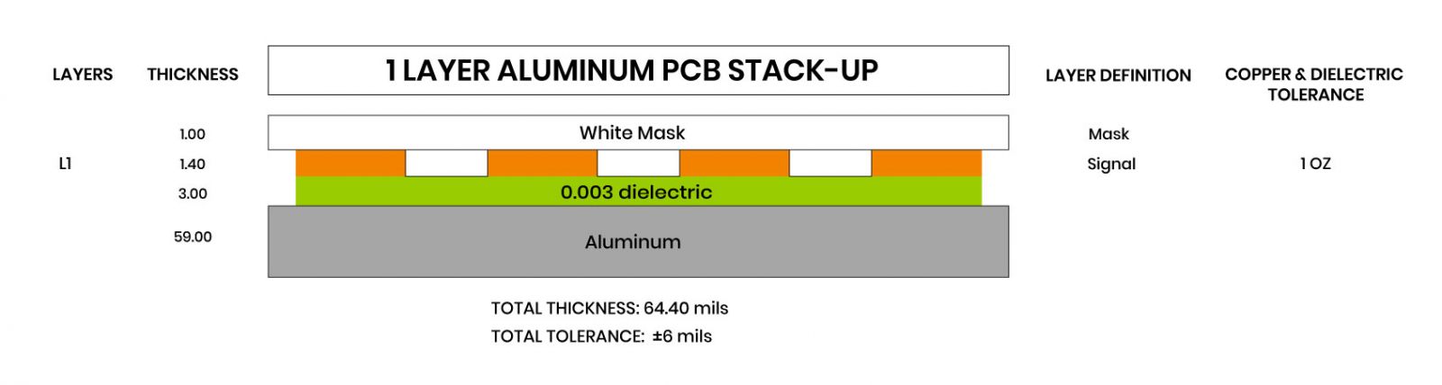
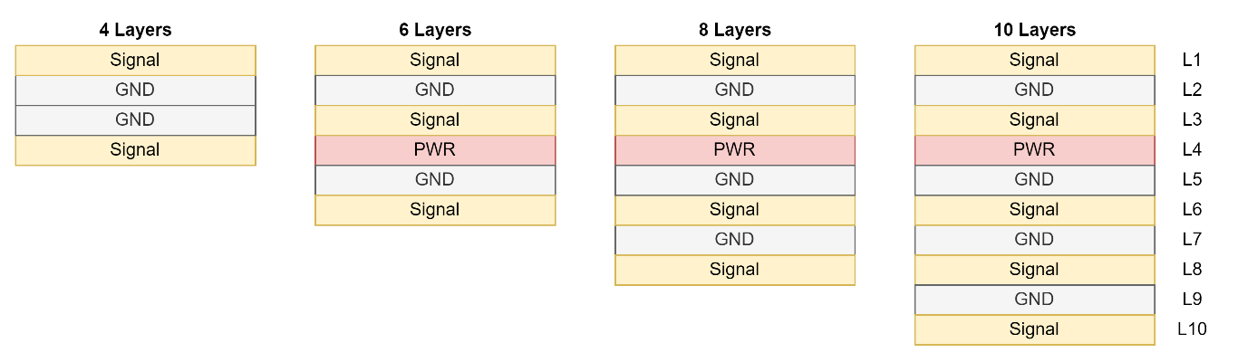
PCB Stack-Up Guide & Examples | San Francisco Circuits
 www.sfcircuits.com
Stack Up Design In Pcb Pcb Design Layout Pcbway | Hot Sex Picture
 www.hotzxgirl.com
High Current PCB: The Perfect Board For High Current Applications
 www.wellpcb.com
Pcb Design High Current 4 Tips On How To Design Pcbs For High Currents
 pcbways.pages.dev
High Current PCB - How To Design And Optimise To Make It More Perfect
 www.ourpcb.com
pcb high current design solder trace removed mask section additional added
PCB Stackup Optimization: Engineering Robust Electronics
 www.wevolver.com
An In-depth Analysis On PCB Stackup - PCBA Manufacturers
 www.pcba-manufacturers.com
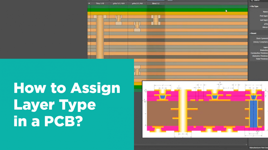
PCB Stackup Explained – How To Plan A Multilayer Stack - IBE Electronics
 www.pcbaaa.com
PCB Stack-up – PCB HERO
 www.pcb-hero.com
Talk About PCB Layer Stackup And PCB Stackup Design - BGPCBA
 bgpcba.com
An In-depth Analysis On PCB Stackup - PCBA Manufacturers
 www.pcba-manufacturers.com
PCB Stack-Up Guide & Examples | San Francisco Circuits
 www.sfcircuits.com
Selecting A PCB Stack-up For EMC Compliance – TechnieX
 techniex.com
PCB Stackup Explained – How To Plan A Multilayer Stack - IBE Electronics
 www.pcbaaa.com
PCB Stack-Up Guide & Examples | San Francisco Circuits
 www.sfcircuits.com
PCB Design For High Currents - Electrical Engineering Stack Exchange
 electronics.stackexchange.com
4 Tips On How To Design PCBs For High Currents - 2023 Updated
 www.pcbonline.com
Pcb Stack Up Impedance Multilayer Pcb Manufacturing Cost
 pcbways.pages.dev
PCB Stackup
 www.nextpcb.com
PCB Stack-Up Guide & Examples | San Francisco Circuits
 www.sfcircuits.com
PCB Stackup Basics - Printed Circuit Boards ‖ Global PCB Solutions
 toptekpcb.com
PCB Stackup Basics - Printed Circuit Boards ‖ Global PCB Solutions
 toptekpcb.com
Selecting a pcb stack-up for emc compliance – techniex. Pcb stackup optimization: engineering robust electronics. Pcb design high current 4 tips on how to design pcbs for high currents