jlcpcb eagle design rules Jlcpcb : advanced pcb design techniques for high-speed signal integrit Pcb techniques
If you are searching about JLCPCB High-precision Multi-layer PCB Extended to 8-20 Layer you've visit to the right web. We have 25 Pics about JLCPCB High-precision Multi-layer PCB Extended to 8-20 Layer like JLCPCB : Advanced PCB Design Techniques for High-Speed Signal Integrit, JLCPCB : Advanced PCB Design Techniques for High-Speed Signal Integrit and also JLCPCB : Advanced PCB Design Techniques for High-Speed Signal Integrit. Here it is:
JLCPCB High-precision Multi-layer PCB Extended To 8-20 Layer
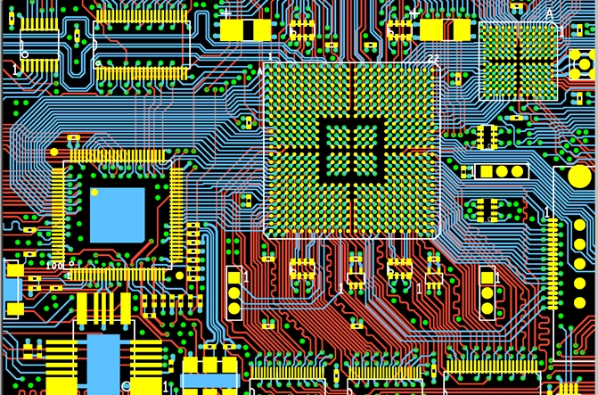
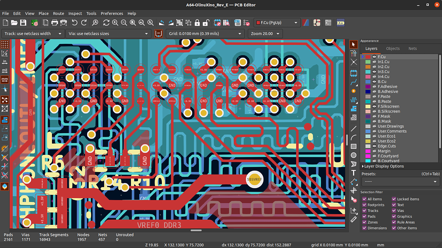
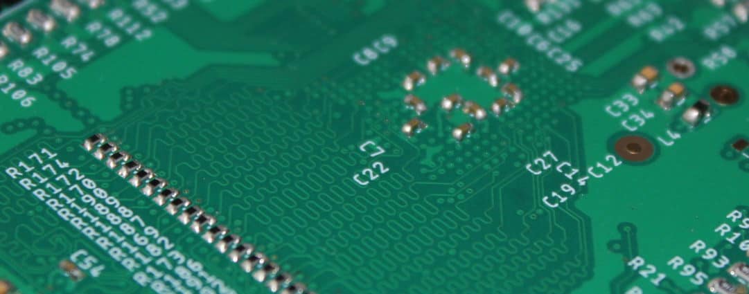
JLCPCB : Advanced PCB Design Techniques For High-Speed Signal Integrit
 jlcpcb.store
Layout Automation Using Advanced PCB Design Techniques - Part 4
 blogs.sw.siemens.com
PCB Design Layout Guidelines For Engineers Advanced PCB Design Blog
 www.designinte.com
JLCPCB : Advanced PCB Design Techniques For High-Speed Signal Integrit
 jlcpcb.store
JLCPCB.com – Eagle Gerber Export And Quick PCB Review - Electronics-Lab.com
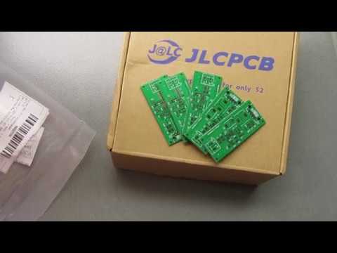 www.electronics-lab.com
jlcpcb eagle export gerber pcb quick review electronics lab
High Speed Pcb Design Archives | TronicsZone
 www.tronicszone.com
pcb techniques
Pcb Design Layout Guidelines Pcb Layout Guidelines For Design
 pcbways.pages.dev
PCB Design Tutorial Using EasyEDA & JLCPCB | PCB Designing
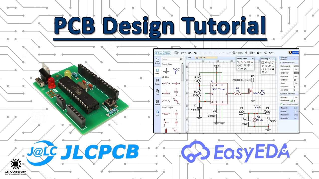 www.circuits-diy.com
pcb easyeda jlcpcb complete circuits electronics
Advancing Your Circuit Design Skills: Tips And Techniques For Improving
JLCPCB.com - Eagle Gerber Export And Quick PCB Review - Electronics-Lab
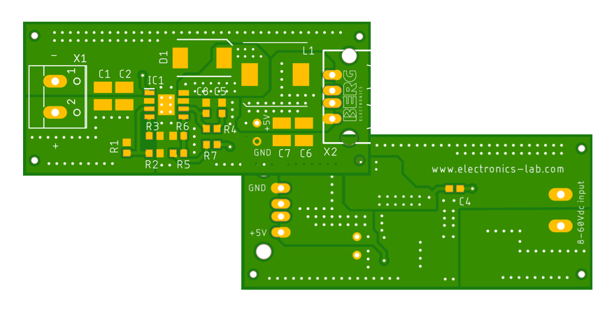 www.electronics-lab.com
pcb gerber jlcpcb eagle
Kicad Jlcpcb Design Rules Kicad Pcb Project Create First
 pcbways.pages.dev
Mastering PCB Routing: Techniques For Optimal Circuit Design And
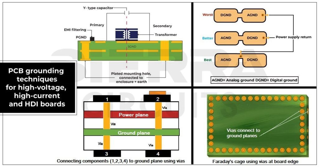
Pcb Design Ground Plane Ground Plane Pcb: A Return Path For Circuit
 pcbways.pages.dev
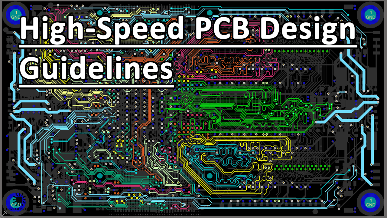
High-Speed PCB Design Guidelines
 circuits-diy.com
pcb circuits techniques diy absolute soldering practices anas ejaz 1843
JLCPCB : Advanced PCB Design Techniques For High-Speed Signal Integrit
 jlcpcb.store
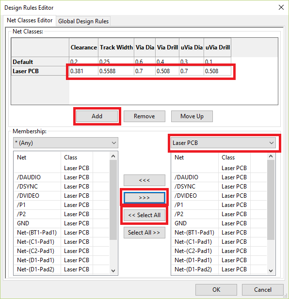
KiCad-DesignRules/JLCPCB/JLCPCB.kicad_dru At Main · Labtroll/KiCad
Mastering PCB Routing: Techniques For Optimal Circuit Design And
Design Rules For JLCPCB - Manufacturing - KiCad.info Forums
 forum.kicad.info
JLCPCB : Advanced PCB Design Techniques For High-Speed Signal Integrit
 jlcpcb.store
【PCB Design Guidance】BGA Design Rules : R/JLCPCB_official
 www.reddit.com
Kicad Jlcpcb Design Rules Kicad Pcb Project Create First
 pcbways.pages.dev
JLCPCB : Advanced PCB Design Techniques For High-Speed Signal Integrit
 jlcpcb.store
Kicad Jlcpcb Design Rules Pcb Designs – Otosection
 otosection.com
High Speed PCB Design Techniques - TronicsZone
 www.tronicszone.com
pcb techniques
Jlcpcb : advanced pcb design techniques for high-speed signal integrit. Mastering pcb routing: techniques for optimal circuit design and. Jlcpcb.com – eagle gerber export and quick pcb review