pcb board circuit diagram Pcb component placement rules Pcb component practices routing circuits 2862
If you are searching about PCB Component placement strategy using Proteus 8 | electronic2017 you've visit to the right web. We have 25 Pics about PCB Component placement strategy using Proteus 8 | electronic2017 like Circuit Board Layout Rules - Circuit Diagram, PCB Component Placement Rules | Sierra Circuits and also Best Rules for PCB Components Placement. Here you go:
PCB Component Placement Strategy Using Proteus 8 | Electronic2017
 electronic2017.blogspot.com
component placement pcb strategy using proteus placed finally shows below figure where was
PCB Component Placement Rules | Sierra Circuits
 www.protoexpress.com
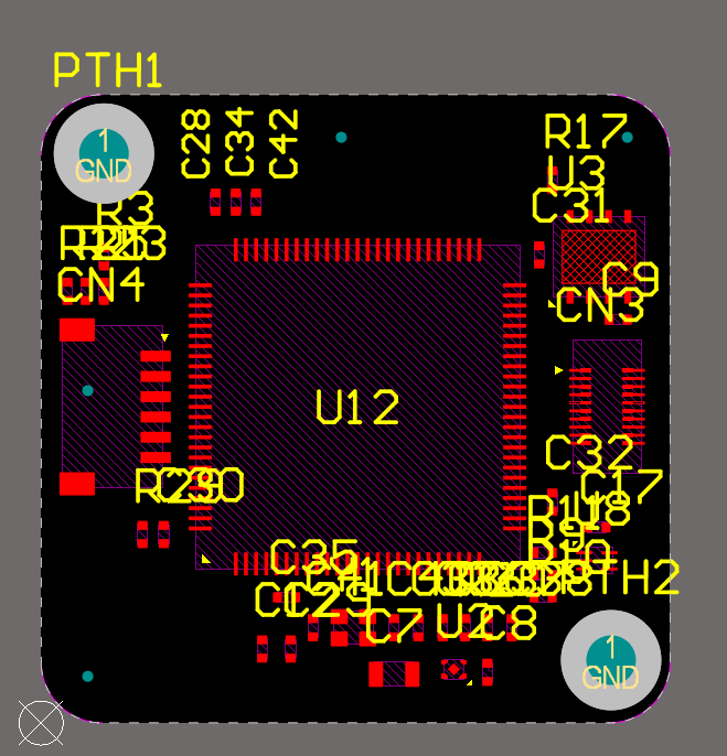
PCB Component Placement | Create Your Own PCB | Video Tutorials | Learn
 my.altium.com
pcb placement component completed layer top altium fig
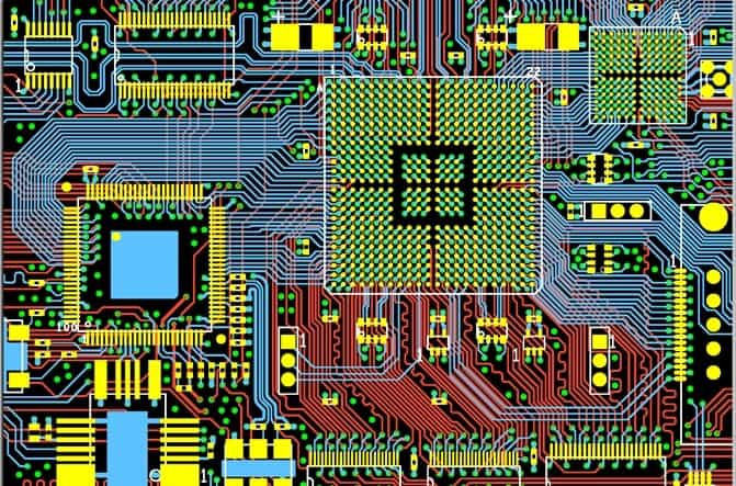
Component Placement Onto The Printed Circuit Board - Engineering
 www.pcbway.com
component placement circuit onto printed board pcbway pcb
Circuit Board Component Diagram Circuit Board Components Par
 arthau3bywiring.z21.web.core.windows.net
PCB Schematic Design - Step By Step Guide | Reversepcb
 reversepcb.com
Circuit Board Layout Rules - Circuit Diagram
 www.circuitdiagram.co
Mastering PCB Layout Design Rules For Optimal Circuit Performance - 86PCB
 86pcb.com
Basic PCB Component Placement Guidelines | Advanced PCB Design Blog
 resources.pcb.cadence.com
Component Placement In PCB Design & Assembly | Sierra Circuits
 www.protoexpress.com
Component Placement Guidelines For PCB Design And Assembly | Sierra
 www.protoexpress.com
placement component blocks circuit pcb design organizing function according figure considerations
Practical PCB Design Layout Rules - Leading PCB Manufacturer - Arisentec®
 arisentecpcb.com
Component Placement In PCB Design & Assembly | Sierra Circuits
 www.protoexpress.com
Basic PCB Component Placement Guidelines | Advanced PCB Design Blog
 resources.ema-eda.com
BASIC PCB Design Rules – Layout
 epci.eu
Top 5 PCB Design Rules You Need To Know – PCB HERO
Component Placement In PCB Design & Assembly | Sierra Circuits
 www.protoexpress.com
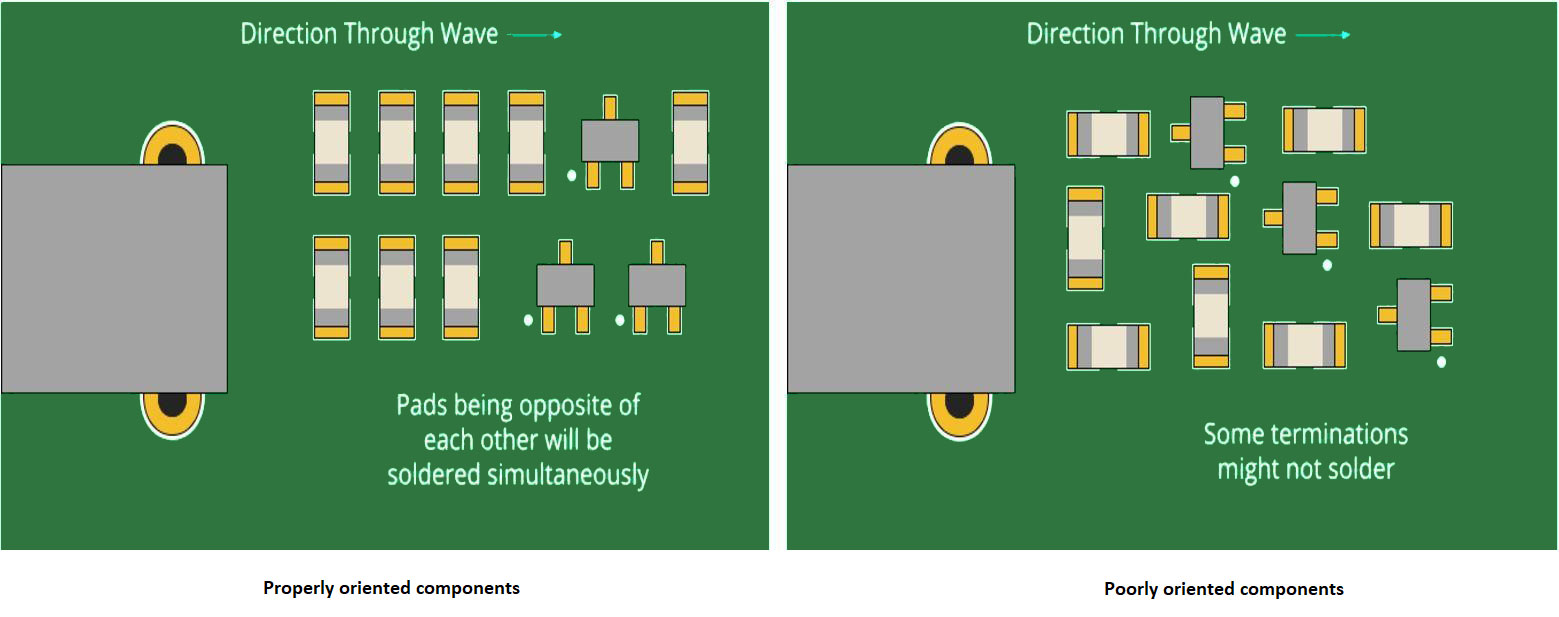
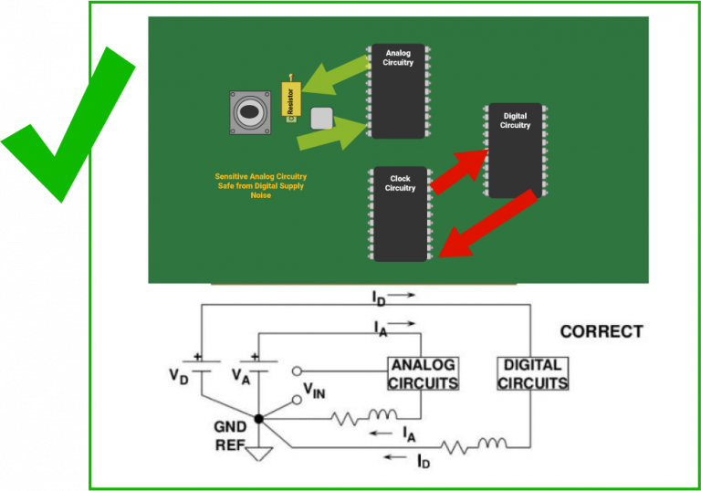
placement pcb component design guidelines assembly good components poor needs designer every know top circuits left right figure
Best Rules For PCB Components Placement
 www.proto-electronics.com
Circuit Board Layout Tips - Circuit Diagram
 www.circuitdiagram.co
PCB Component Placement: A Comprehensive Guide
 www.elepcb.com
Component Placement On A PCB – A Step-By-Step Guide - Miracle
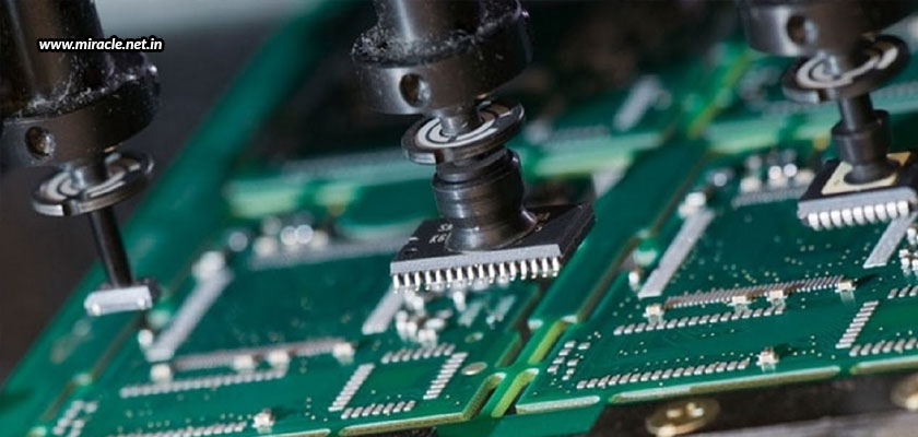 www.miracle.net.in
pcb component placement step guide circuit miracle electronics
PCB Component Placement Guidelines - Tips & Tricks
 www.circuits-diy.com
pcb component practices routing circuits 2862
PCB Walk-through 3: Component Placement | EMA Design Automation
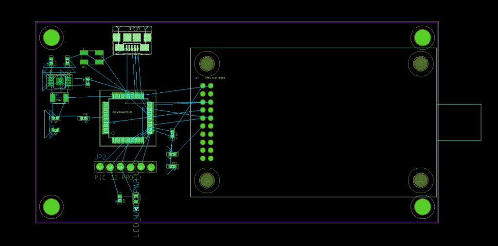 www.ema-eda.com
PCB Walk-through 3: Component Placement | EMA Design Automation
 www.ema-eda.com
PCB Component Placement | Create Your Own PCB | Video Tutorials | Learn
 my.altium.com
pcb placement component layer completed bottom altium fig
Pcb component placement guidelines. Component placement circuit onto printed board pcbway pcb. Basic pcb design rules – layout