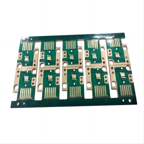
pcb copper layout desolved board 3,059 copper on pcb images, stock photos, 3d objects, & vectors
If you are searching about How to remove copper from PCB board? - PCBBUY.COM you've visit to the right web. We have 25 Pics about How to remove copper from PCB board? - PCBBUY.COM like Maximizing Copper: Design Considerations for Printed Circuit Boards, How to Make Copper-Clad Boards With the Best PCB Layout Software and also [Solved] PCB Layout Review | SolveForum. Here it is:
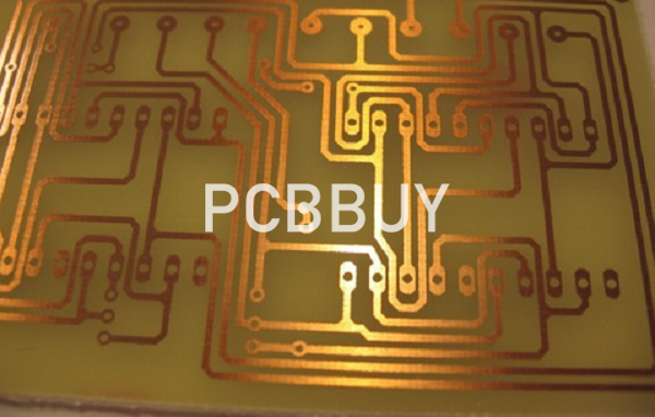
How To Remove Copper From PCB Board? - PCBBUY.COM
 www.pcbbuy.com
pcb stripped
[Solved] PCB Layout Review | SolveForum
![[Solved] PCB Layout Review | SolveForum](https://i.stack.imgur.com/q0rtA.png) www.solveforum.com
www.solveforum.com
6 Common Problems In PCB Design – Layout – Olinapcb
 olinapcb.com
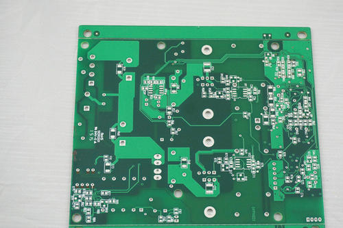
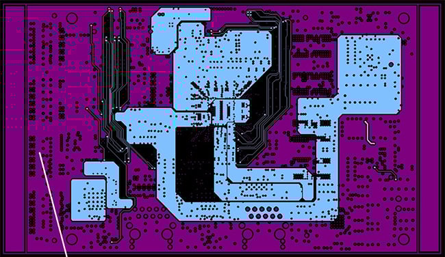
PCB Layout, Copper Side | Download Scientific Diagram
 www.researchgate.net
PCB Circuit Board Copper Deposition Process Flow_Company News_News_KnownPCB
 www.knownpcb.com
Unconnected Copper - PCB Design - PCB Design & IC Packaging (Allegro X
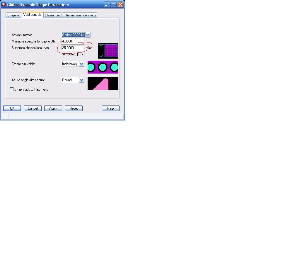 community.cadence.com
[Solved] PCB Layout Review | SolveForum
![[Solved] PCB Layout Review | SolveForum](https://i.stack.imgur.com/YdhdG.png) www.solveforum.com
www.solveforum.com
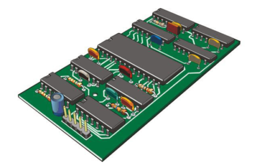
Maximizing Copper: Design Considerations For Printed Circuit Boards
 www.scribd.com
Printed Layout Structure Of PCB On Copper Laminate | Download
 www.researchgate.net
laminate pcb layout
FPGA Breakout Board Layout – Skywired.net
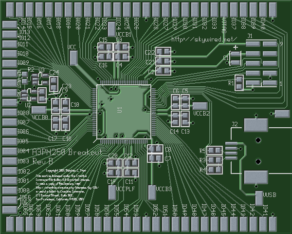 skywired.net
fpga breakout pcb layout top board side
3,059 Copper On Pcb Images, Stock Photos, 3D Objects, & Vectors
 www.shutterstock.com
Routing - PCB Design Considerations - Copper Pouring - Electrical
 electronics.stackexchange.com
pcb copper pouring considerations design
Microcontroller - PCB Layout Questions For MCU Breakout Board
 electronics.stackexchange.com
pcb layout board breakout mcu questions stack
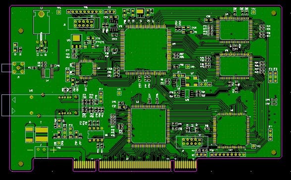
PCB Layout | Details | Hackaday.io
 hackaday.io
PCB Single-Sided (S-S) / Double-Sided (D-S) Pure Copper Clad Laminate
 shop.techmakers.com.my
Optimize Performance With High-Quality Copper Printed Circuit Boards
 sfxpcb.com
PCB Layout | Details | Hackaday.io
 hackaday.io
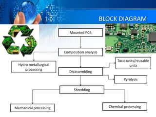
E-WASTE MANAGEMENT (COPPER RECOVERY FROM PCB) | PPT
 www.slideshare.net
Single Side Copper Prototype Pcb Universal Board 12x18 Cm - Rytronics.in
 www.rytronics.in
Thermoelectric Separation Copper Based PCB - Best PCB
 bestpcb-ems.com
How To Make Copper-Clad Boards With The Best PCB Layout Software
 resources.altium.com
Schematic Of The Designed PCB (Top Copper, Bottom Copper) | Download
 www.researchgate.net
3,059 Copper On Pcb Images, Stock Photos, 3D Objects, & Vectors
 www.shutterstock.com
Summary Of PCB Layout And Routing Skills – Olinapcb
 olinapcb.com
pcb routing summary thickness
Balancing Layers In Your PCB Layout
 blog.epectec.com
pcb reduce poured copper balancing
Pcb layout. Pcb layout board breakout mcu questions stack. Balancing layers in your pcb layout