pcb design and fabrication pdf Basic steps to design a pcb layout Pcb fabrication terbaru skema gaya
If you are searching about PCB Design Tutorial | PDF | Printed Circuit Board | Electronic Circuits you've came to the right page. We have 25 Images about PCB Design Tutorial | PDF | Printed Circuit Board | Electronic Circuits like PCB Layout Design | PDF, PCB Design | PDF and also How to Design a PCB Layout | Sierra Circuits. Here it is:
PCB Design Tutorial | PDF | Printed Circuit Board | Electronic Circuits
 www.scribd.com
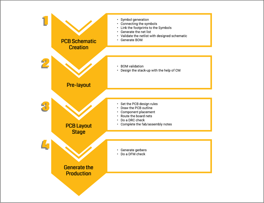
Pcb Designing How To Design A Pcb Step By Step – Artofit
 www.artofit.org
Pcb Design Steps - Design Talk
 design.udlvirtual.edu.pe
Pcb Layout Vs Schematic Design Pdf » Wiring Diagram
 www.organised-sound.com
PCB Layout Design | PDF
 www.scribd.com
Pcb Designing How To Design A Pcb Step By Step – Artofit
 www.artofit.org
PCB Assembly - Circuit Board Assembly Process
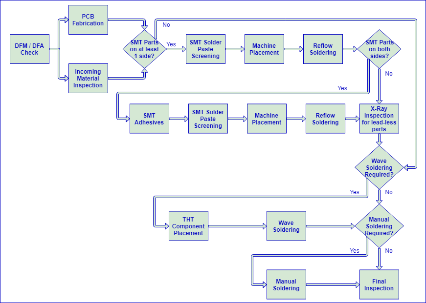 www.7pcb.com
Practical PCB Design Layout Rules - Leading PCB Manufacturer - Arisentec®
 arisentecpcb.com
Pcb Layout Design Image Download – Artofit
 www.artofit.org
PCB Design | PDF
 www.scribd.com
Pcb Layout Design The Basics By PCBCART - Issuu
 issuu.com
Stream Read ️ PDF PCB Design And Layout Fundamentals For EMC By Roger
 soundcloud.com
How To Design PCB Board: A Step-by-step Guide For PCB Design
 www.pcbasic.com
PCB Design For Manufacture [PDF] - Electronics-Lab.com
![PCB Design for manufacture [PDF] - Electronics-Lab.com](https://www.electronics-lab.com/wp-content/uploads/2017/05/1.jpg) www.electronics-lab.com
www.electronics-lab.com
pcb manufacture
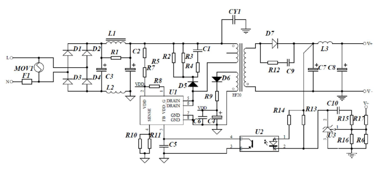
PCB Layout Design | PDF | Capacitor | Analogue Electronics
 www.scribd.com
(PDF) PCB Design And Fabrication Process - DOKUMEN.TIPS
 dokumen.tips
Mastering PCB Layout Design Rules For Optimal Circuit Performance - 86PCB
 86pcb.com
Guide To PCB Design | PDF | Computer Engineering | Electrical Engineering
 www.scribd.com
Complete Guide To PCB Layout Design: Tips, Basics, & Guidelines
 sfxpcb.com
Gaya Terbaru Pcb Design Steps, Skema Pcb
 skemadriver.blogspot.com
pcb fabrication terbaru skema gaya
Basic Steps To Design A PCB Layout – PCB HERO
 www.pcb-hero.com
Teknik Pembuatan Layout PCB Secara Manual | PDF
 id.scribd.com
PCB Designing - How To Design A PCB (Step By Step) | PDF | Printed
 www.scribd.com
(PDF) PCB Design And Fabrication Tutorial - DOKUMEN.TIPS
 dokumen.tips
How To Design A PCB Layout | Sierra Circuits
 www.protoexpress.com
pcb design layout process flowchart schematic software
Pcb design tutorial. Pcb designing how to design a pcb step by step – artofit. Pcb manufacture