pcb design lab manual Pcb design guide Pcb manual
If you are looking for PCB Design Process | ALLPCB you've came to the right place. We have 25 Pictures about PCB Design Process | ALLPCB like Guide to PCB Design | PDF | Computer Engineering | Electrical Engineering, PCB Manual | PDF and also PCB Design Practical-Full Wave Rectifier - Androiderode. Read more:
PCB Design Process | ALLPCB
 www.allpcb.com
pcb design allpcb knowledge basic process
PCB Design Final | PDF
 www.scribd.com
PCB Design Practical-Full Wave Rectifier - Androiderode
 www.androiderode.com
pcb design rectifier wave full practical multisim androiderode layout transfer single side
Pcb Design Guide - PCB Design By DL Designs
 dl-designs.co.uk
Pcb Design Lab - PCB LAB MANUAL - Electronics & Communication
 www.studocu.com
Ten Golden Rules: Best Practices For Optimizing PCB Design – GREATPCB
 greatpcb.com
PCB Design Basics | PDF | Printed Circuit Board | Electromagnetic
 www.scribd.com
PCB Manual | PDF
 www.scribd.com
Practical PCB Design Layout Rules - Leading PCB Manufacturer - Arisentec®
 arisentecpcb.com
PCB DESIGN - EasyEDA Open Source Hardware Lab
 oshwlab.com
PCB - Design Guidlines PDF | PDF | Electronic Component | Printed
 www.scribd.com
PCB Design Method And PCB Design Steps - Kingford
 www.kingfordpcb.com
PCB Design Practical-Full Wave Rectifier
 www.androiderode.com
pcb simulation rectifier design wave full circuit practical androiderode button run test
Gaya Terbaru Pcb Design Steps, Skema Pcb
 skemadriver.blogspot.com
pcb fabrication terbaru skema gaya
PCBDesign Studio Tutorial | PDF | Electrical Engineering | Computer Science
 www.scribd.com
Pcb Design Guide - PCB Design By DL Designs
 dl-designs.co.uk
Guide To PCB Design | PDF | Computer Engineering | Electrical Engineering
 www.scribd.com
PCB Design Practical-Full Wave Rectifier
 www.androiderode.com
pcb rectifier practical design androiderode wave full
Mastering PCB Layout Design Rules For Optimal Circuit Performance - 86PCB
 86pcb.com
Pcb Design - EasyEDA Open Source Hardware Lab
 oshwlab.com
PCB Design Tutorial | PDF | Printed Circuit Board | Electronic Circuits
 www.scribd.com
How To Design Your Own PCB - From Basic Layout Tips To Final Artwork
 www.raypcb.com
PCB Design | PDF
 www.scribd.com
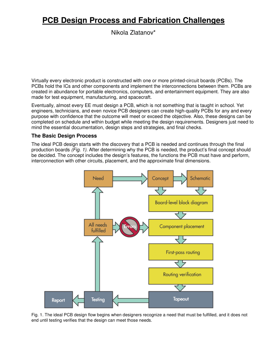
(PDF) PCB Design
 www.researchgate.net
Mechanical PCB Design | Mechanics
 mechanics.co.il
pcb mechanical design mechanics layout
Pcb design rectifier wave full practical multisim androiderode layout transfer single side. Pcb design lab. Pcb fabrication terbaru skema gaya