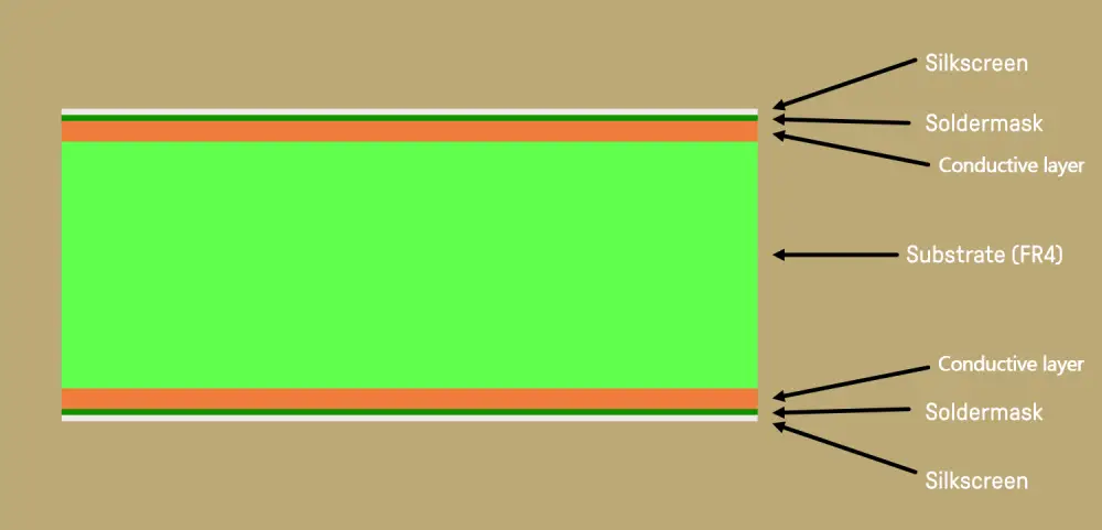
pcb layer structure What is any layer pcb and how is it produced?
If you are searching about Layer 3 of main PCB. | Download Scientific Diagram you've visit to the right place. We have 25 Pics about Layer 3 of main PCB. | Download Scientific Diagram like What Makes Two Layers PCB Popular - ALLPCB.com - ALLPCB.com, PCB structure : A detailed introduction to its layers - IBE Electronics and also PCB Layers & printed circuit board working Layers – ALLPCB.com. Here you go:
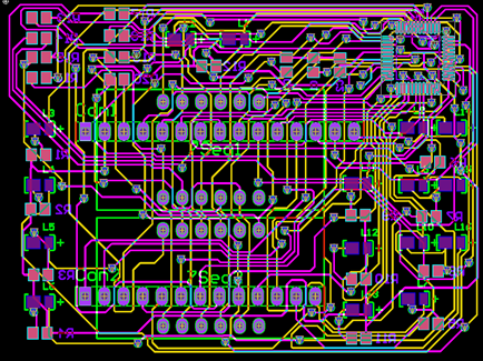
Layer 3 Of Main PCB. | Download Scientific Diagram
 www.researchgate.net
What Makes Two Layers PCB Popular - ALLPCB.com - ALLPCB.com
 www.allpcb.com
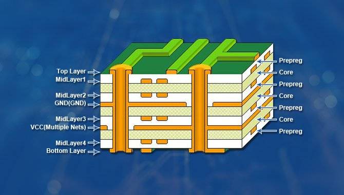
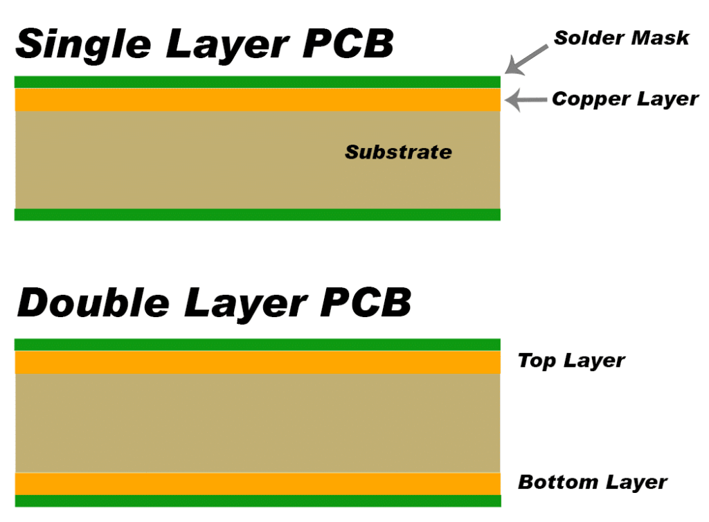
pcb two layers structure layer allpcb
The Meaning Of Each Layer Of PCB Board - PCBA Manufacture
 www.dyc-electronic.com
What Is Any Layer PCB And How Is It Produced? | Viasion
 www.viasion.com
PCB Board Layers
 mungfali.com
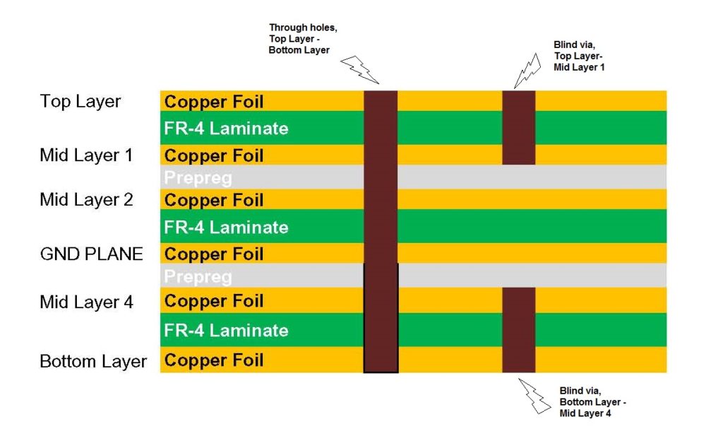
Designing A 6-Layer PCB Stackup For Enhanced EMC Blog, 48% OFF
.png) www.oceanproperty.co.th
www.oceanproperty.co.th
Understanding Double Layer PCB - PCBA Manufacturers
 www.pcba-manufacturers.com
PCB Layer Design To Follow The Principles - Kingford
 www.kingfordpcb.com
Pcb Layers: Over 1,696 Royalty-Free Licensable Stock Photos | Shutterstock
 www.shutterstock.com
A Must Read: PCB Material Guide - MOKO Technology
 www.mokotechnology.com
PCB Circuit Board Structure Of The Even-numbered Layers Of PCBs
 www.circuitwork.tech
pcb layers pcbs
What Is The Layer Of A PCB?
 www.linkedin.com
How To Determine PCB Layers
 hillmancurtis.com
The Basics Of PCB Layers
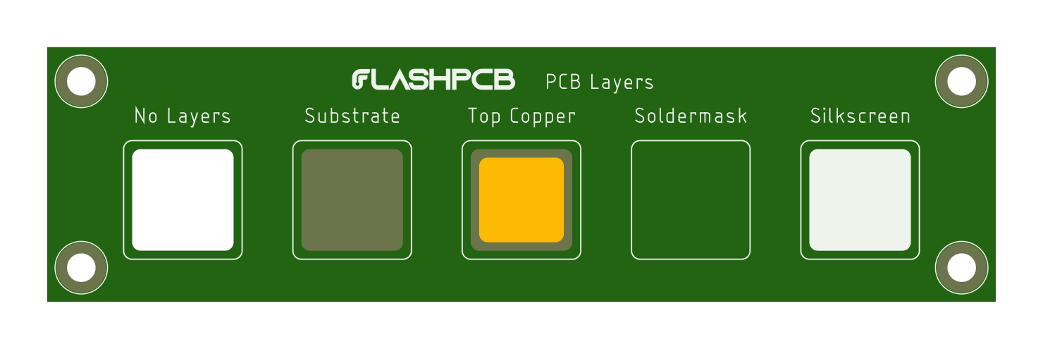 www.flashpcb.com
PCB Fabricate - PCBA Manufacture
 www.dyc-electronic.com
PCB Layers & Printed Circuit Board Working Layers – ALLPCB.com
 www.allpcb.com
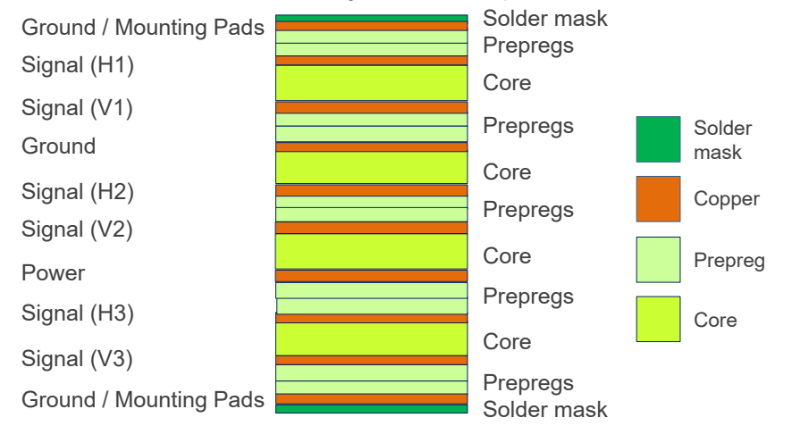
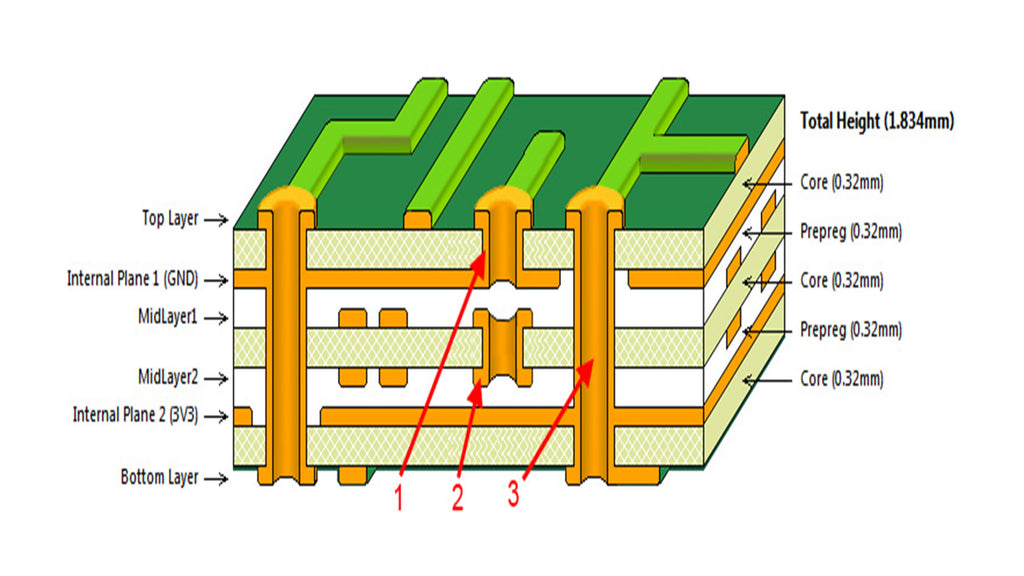
pcb layers layer board impedance circuit stackup stack printed signal plane thickness altium internal allpcb copper working
PCB Layer Stack-Up: A Comprehensive Overview
 www.nextpcb.com
Guide To Six-Layer PCB Stack-up And Manufacturing Process | Viasion
 www.viasion.com
Exploring The Layers Of A PCB: Composition And Structure Unveiled
 www.linkedin.com
PCB Layers Explained: Everything You Need To Know
 www.fscircuits.com
12 Layer PCB: A Guide To Frequently Asked Questions
 www.venture-mfg.com
Layer 4 Of Main PCB. | Download Scientific Diagram
 www.researchgate.net
PCB Structure : A Detailed Introduction To Its Layers - IBE Electronics
 www.pcbaaa.com
Complete Guide: How To Choose The Most Suitable Layer Number For PCB
 top10pcb.com
pcb layer sided jenis fr4 stackup wellpcb pengertian fungsi concevoir disposition beserta perlu ketahui anda suitable traces
Important Considerations While Designing A Multi-Layer Board – PCB HERO
 www.pcb-hero.com
Understanding double layer pcb. Pcb layers & printed circuit board working layers – allpcb.com. Pcb layer design to follow the principles