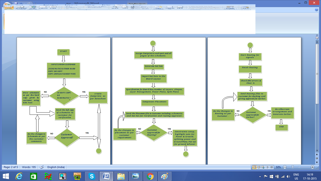
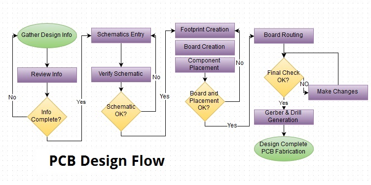
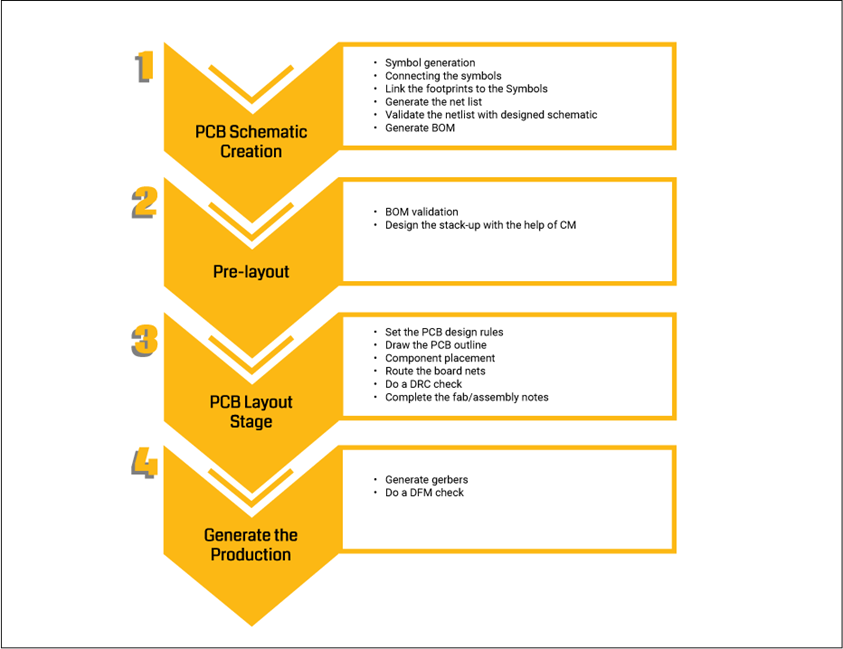
pcb layout design flow chart Pcb design flow wiwo layout offered services tech
If you are looking for WIWO Technologies you've visit to the right page. We have 25 Pictures about WIWO Technologies like PCB Layout Design | PDF, PCB Layout & Design and also PCB Layout – E-slate. Read more:
WIWO Technologies
 www.wiwo-tech.com
pcb design flow wiwo layout offered services tech
PCB Layout Design | PDF
 www.scribd.com
PCB Layout Design - Image Download | Electronic Circuit Design, Layout
 www.pinterest.com
Pcb Design Flow Chart - IMAGESEE
 imagesee.biz
PCB Flow Chart: From Design To Assembly - VSE
 www.vse.com
PCB Layout Design - RaceEL Systems
 www.raceelsystems.com
Complete Guide To PCB Layout Design: Tips, Basics, & Guidelines
 sfxpcb.com
Pcb Design Flow Chart - IMAGESEE
 imagesee.biz
PCB Layout Design - Dynamic Circuit Group Design
 dgcdinc.com
Pcb Design Layout Guidelines Pcb Layout Guidelines For Design
 pcbways.pages.dev
PCB Layout Design – Twinkle Technology
 twinkle.com.my
pcb twinkle
PCB Layout Services| PCB Prototype | Reverse Engineering
 gespcb.com
SEM 1/2013: Circuit Design Part 2 : PCB Layout
 fypikhairiani.blogspot.com
Process - Wellerpcb.com
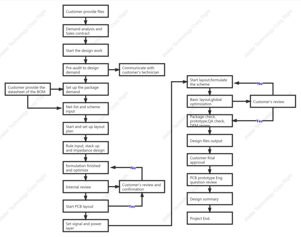 wellerpcb.com
Custom PCB Design & Layout
 mitsi.com
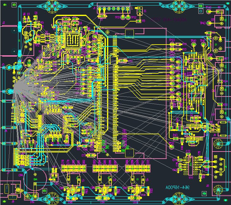
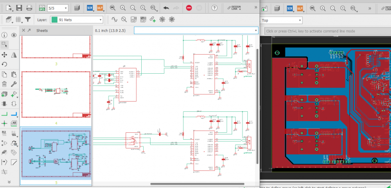
PCB Layout & Design
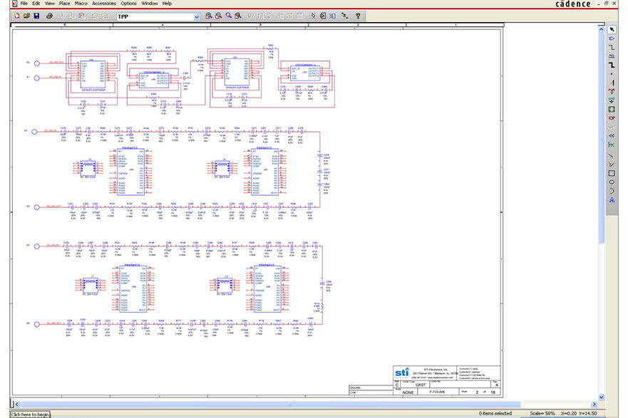 stiusa.com
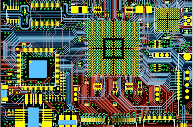
pcb
PCB Design-DTE Electronics Pte Ltd
 dte-electronics.com
PCB Design & Layout
 www.truelancer.com
Pcb Layout | Model Scenery Tutorials
 steamtraininfo.com
Pcb Design Pcb Layout And Circuit Design | Upwork
 www.upwork.com
Pcb Design Flow Chart - IMAGESEE
 imagesee.biz
PCB Layout – E-slate
 eslatetech.com
The Ultimate Guide To PCB Layout Design
Pcb Layout Design Pcb Assembly Pcb Manufacturing Pcb Design Ourpcb
 www.bank2home.com
Basic Steps To Design A PCB Layout – PCB HERO
 www.pcb-hero.com
Pcb layout – e-slate. Pcb layout design. Wiwo technologies