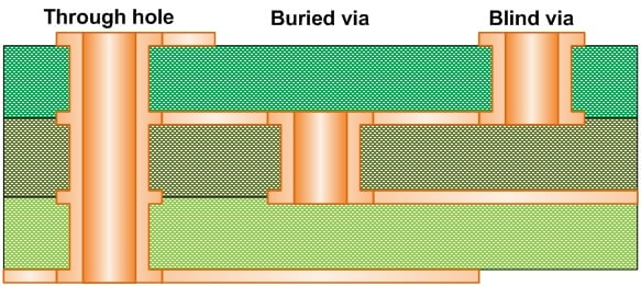
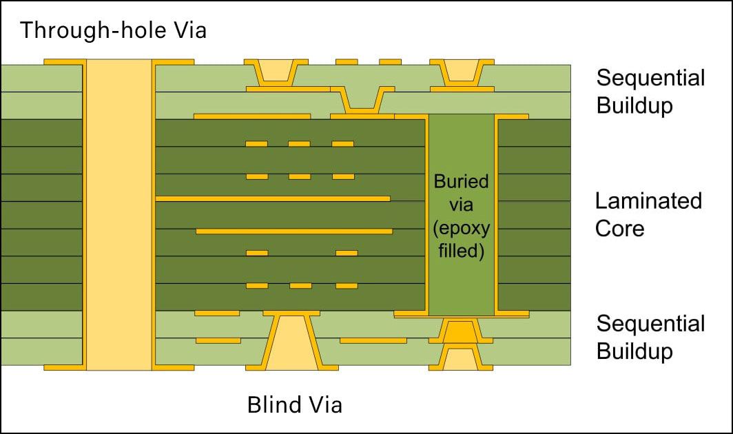
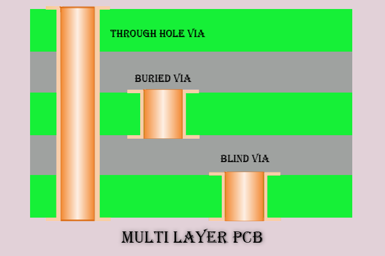
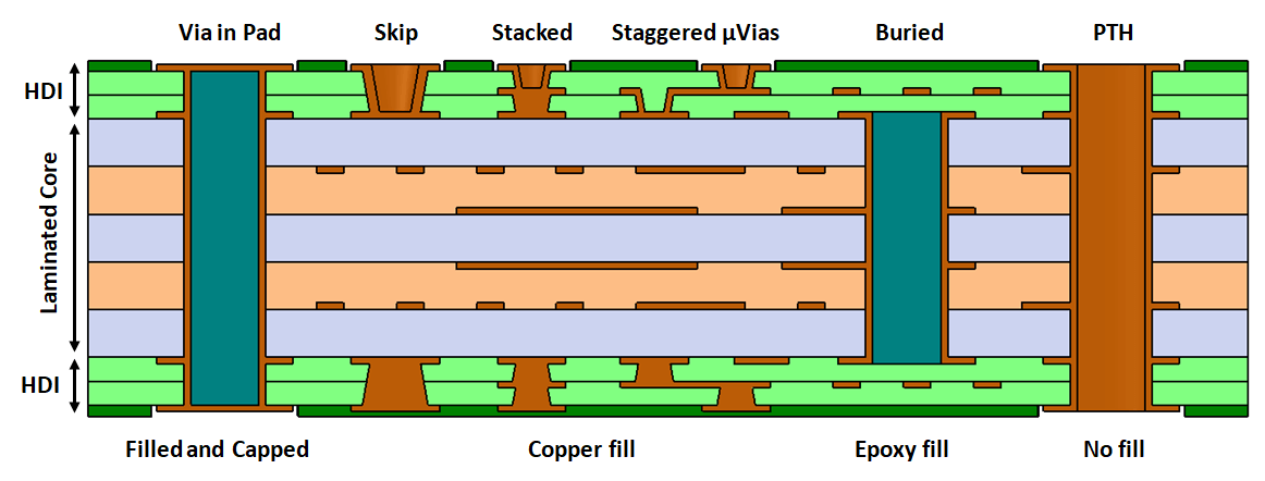
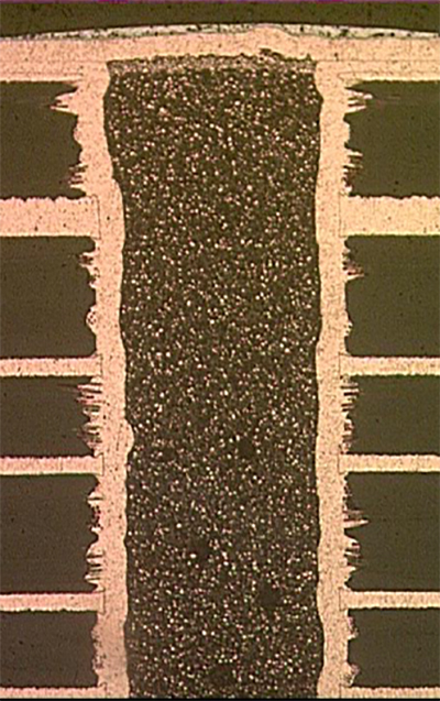
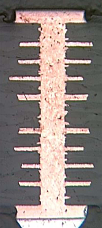
via hole in pcb Pcb vias: an in-depth guide Understanding blind, buried, and through-hole vias in pcb
If you are looking for pcb standard hole sizes How to choose a pcb board size you've came to the right page. We have 25 Pictures about pcb standard hole sizes How to choose a pcb board size like PCB Vias: An In-Depth Guide (2022), PCB Vias: An In-Depth Guide (2022) and also A Complete Guide to Vias in PCB Design - Electronics Post. Read more:
Pcb Standard Hole Sizes How To Choose A Pcb Board Size
 pcbways.pages.dev
Plated Through-Hole Vias In MmWave PCBs | PCB Design Blog | Altium Designer
 resources.altium.com
How And Where Use Vias In PCB Design
 www.proto-electronics.com
How Are PCB Vias Plated? - VSE
 www.vse.com
Aksesoris Pcb Via, Skema Pcb
 skemadriver.blogspot.com
pcb multilayer vias pcbs aksesoris skema advantages manufacture solderless allpcb substrate javatpoint allaboutcircuits
What Is Via In PCB Design And How To Use Them - Gadgetronicx
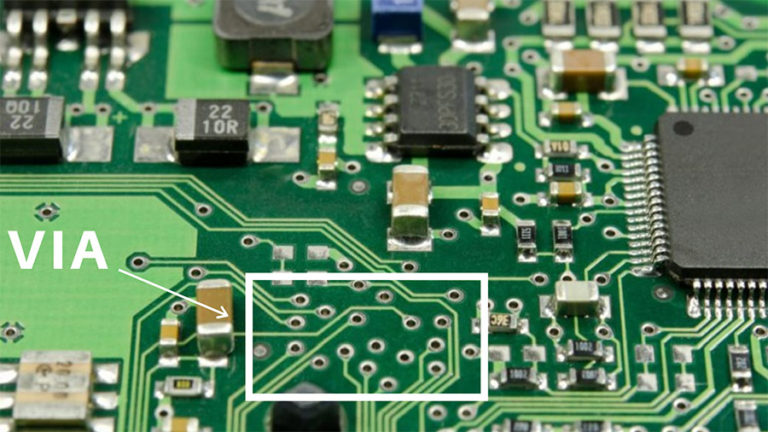 www.gadgetronicx.com
pcb gadgetronicx
Via PCB Design Guide: Which Type Is Best For You?
 hillmancurtis.com
3 Treatment Methods For PCB Vias - Printed Circuit Board Manufacturing
 www.raypcb.com
pcb vias printed
PCB Plated Shut Through Hole Vias - Circuit Board Process Methods
 www.epectec.com
vias plated shut pcb copper hole through circuit board actual
PCB Via: An Ultimate Guide
 www.nextpcb.com
PCB Via Design | Sierra Circuits
 www.protoexpress.com
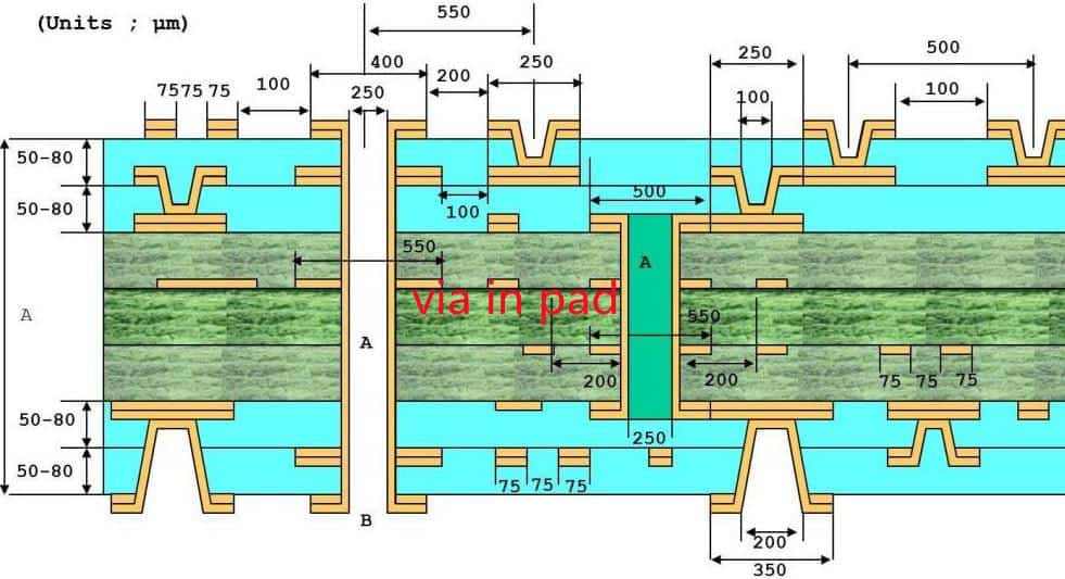
Introduction To Via Types- Buried And Blind Vias And Through-hole And
 pcbassemblymanufacturing.com
Understanding Blind, Buried, And Through-hole Vias In PCB
 circuitdigest.com
pcb vias buried blind understanding debashis das
Through Hole Pcb Board Pcb Copper Core Hole Through Metal Bare Assembly
 pcbways.pages.dev
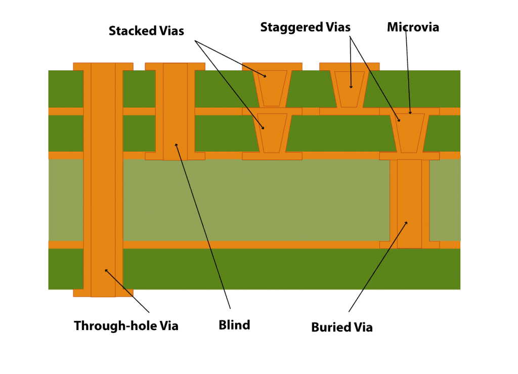
Different Types Of PCB Via - Through-hole, Blind, Buried, Micro Vias
 www.flux.ai
Pcb Thermal Via Hole - Claire Trend
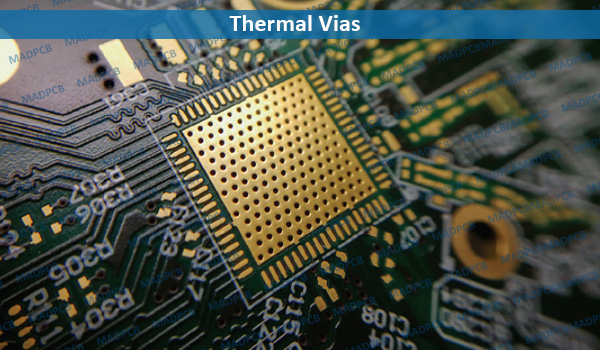 claire-trends.blogspot.com
PCB Vias: An In-Depth Guide
 www.epiccolo.com
PCB Vias - Everything You Need To Know
 blog.epectec.com
pcb via vias treatments everything need know blog
PCB Vias: An In-Depth Guide (2022)
 birthdaywishes77.com
How And Where Use Vias In PCB Design
 www.proto-electronics.com
PCB Vias: An In-Depth Guide (2022)
 itchol.com
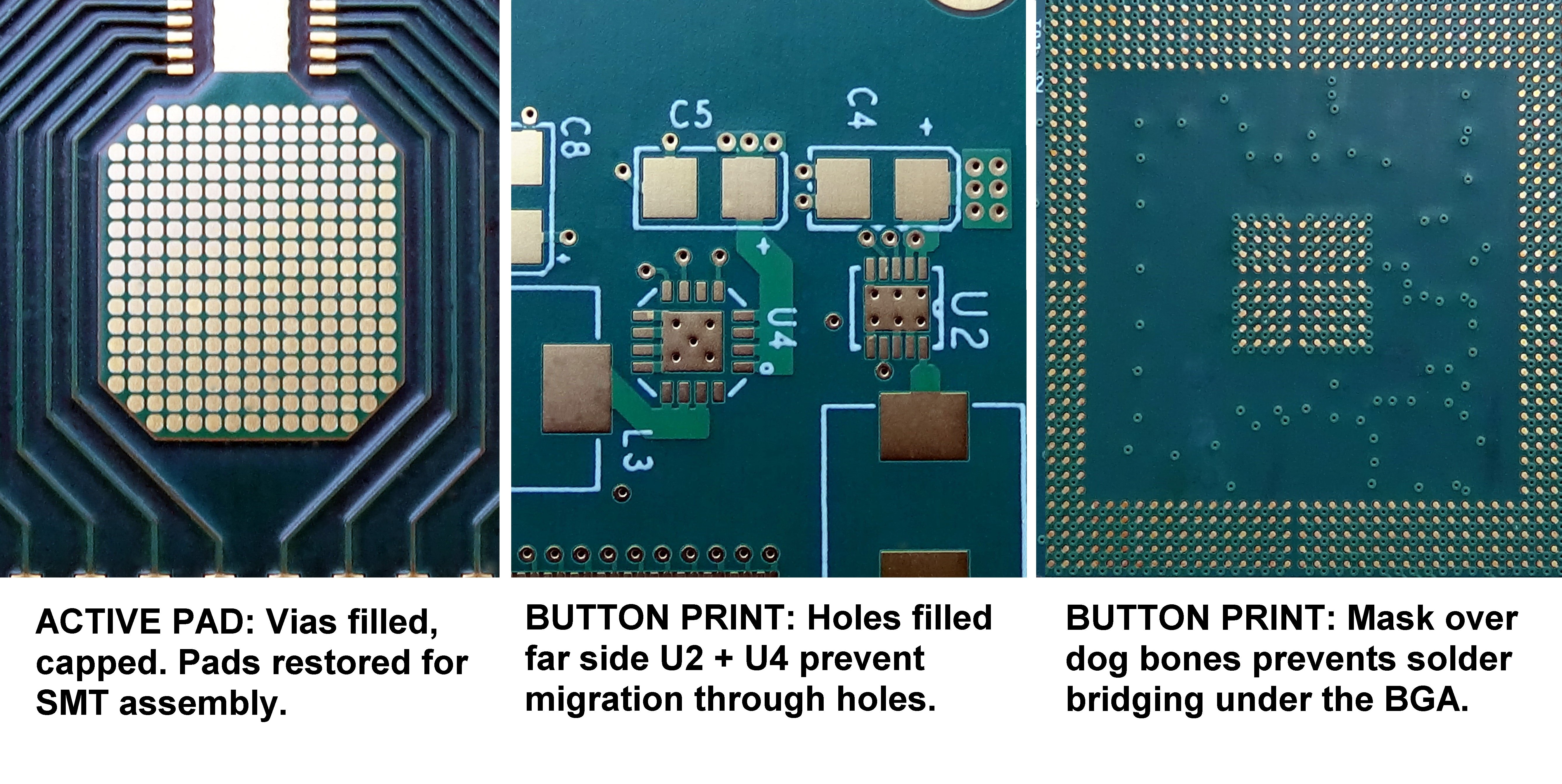
PCB Vias Filling - Conductive, Non-Conductive, And Copper-Plated Shut
 www.epectec.com
PCB Vias Filling - Conductive, Non-Conductive, And Copper-Plated Shut
 www.epectec.com
What Are Tented Vias? A Guide To This Important PCB Feature - JHYPCB
 www.pcbelec.com
A Complete Guide To Vias In PCB Design - Electronics Post
 electronicspost.com
pcb vias design barrel hole complete guide layer metal
Different types of pcb via. 3 treatment methods for pcb vias. Pcb standard hole sizes how to choose a pcb board size