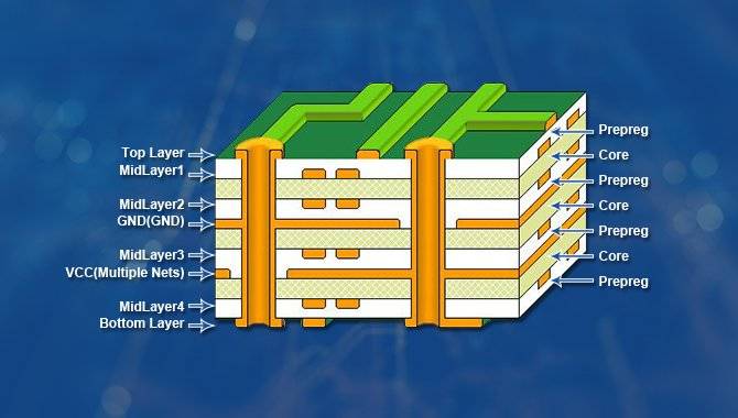
pcb lay up structure Complete guide to pcb layout design steps and rules
If you are looking for 5-layer PCB - Everything You Need to Know - PCBA Manufacturers you've visit to the right page. We have 25 Pictures about 5-layer PCB - Everything You Need to Know - PCBA Manufacturers like PCB structure : A detailed introduction to its layers - IBE Electronics, PCB Layup Design Advantages of Multilayer PCB and also 6 Layer PCB Stackup, Thickness, Impedance Control PCB & MCPCB – Best. Here you go:
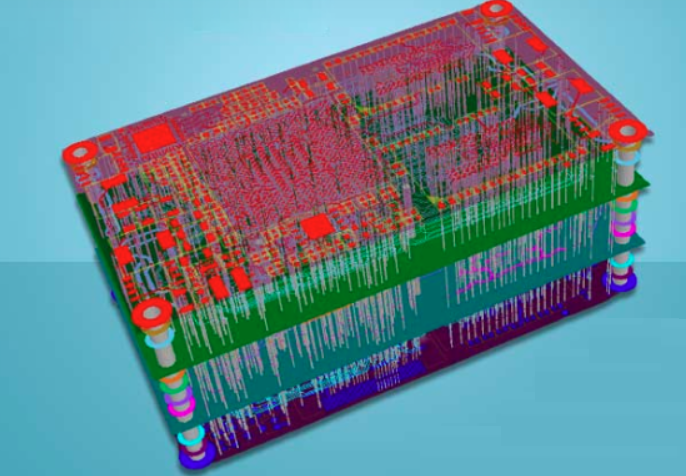
5-layer PCB - Everything You Need To Know - PCBA Manufacturers
 www.pcba-manufacturers.com
6 Layer PCB Stackup, Thickness, Impedance Control PCB & MCPCB – Best
 www.bestpcbs.com
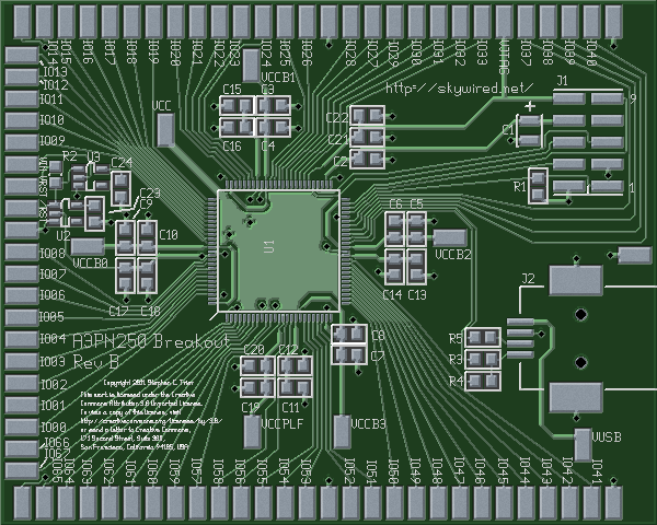
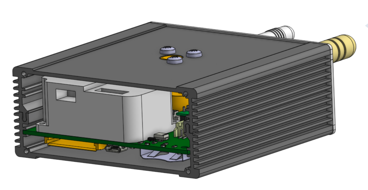
FPGA Breakout Board Layout – Skywired.net
 skywired.net
fpga breakout pcb layout top board side
PCB Fabricate - PCBA Manufacture
 www.dyc-electronic.com
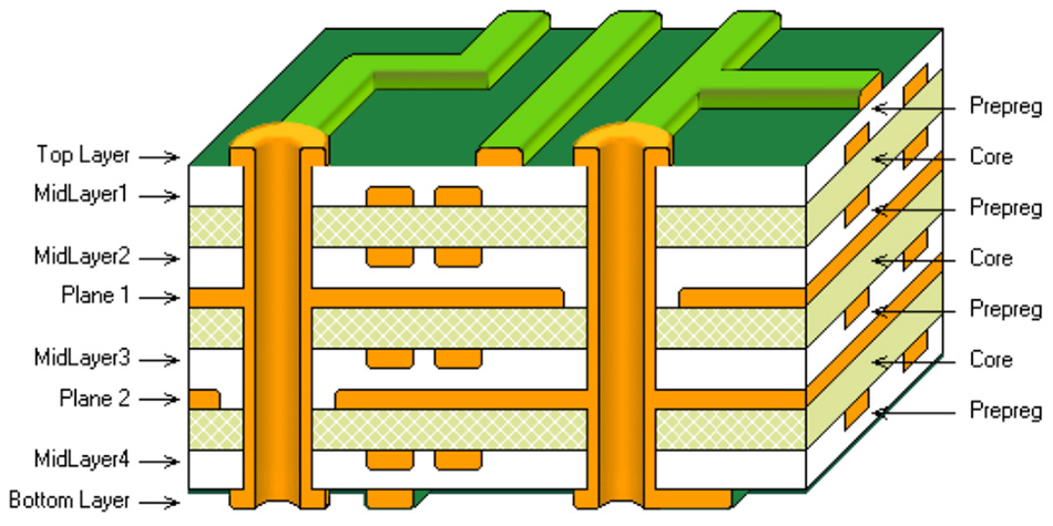
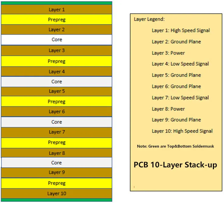
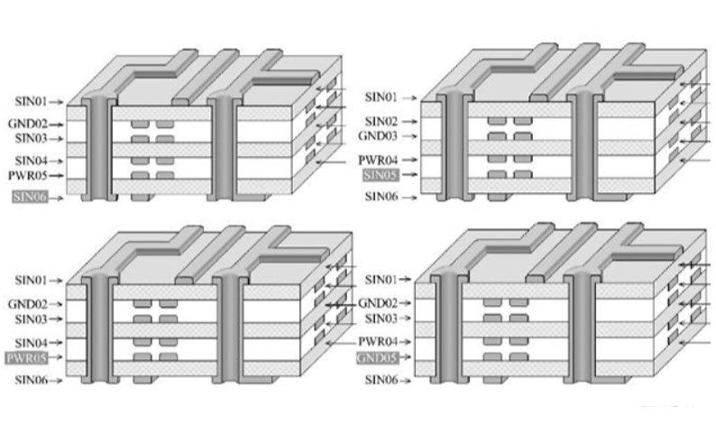
PCB Basics 2: Design Guidelines
PCB Structure : A Detailed Introduction To Its Layers - IBE Electronics
 www.pcbaaa.com
PCB Design Basics: From Schematic To Board Layout - Full Stop India
 www.fullstopindia.com
PCB Layout | Details | Hackaday.io
 hackaday.io
PCB Layout | Details | Hackaday.io
 hackaday.io
What Is PCB Stackup? - PCBBUY.COM
 www.pcbbuy.com
Tips For PCB Layout Service - Engineering Your Ideas Into Reality
 gespcb.com
Aluminum PCB - Low-cost Aluminum PCB Manufacturer China | Viasion
 www.viasion.com
Basic PCB Layer Stackup Design Guidelines - TechSparks
 www.tech-sparks.com
PCB Layer Stack Up And Rules To Properly Design - Jarnistech
 www.jarnistech.com
6 Layerpcb | PCB & MCPCB - Best Technology PCB & MCPCB – Best Technology
 www.bestpcbs.com
PCB Stack Up Guide - Wellerpcb.com
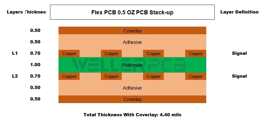 wellerpcb.com
Complete Guide To PCB Layout Design: Tips, Basics, & Guidelines
 sfxpcb.com
Determining PCB Via Size [w/ Guidelines]
![Determining PCB Via Size [w/ Guidelines]](https://www.cirexx.com/wp-content/uploads/PCB-Layout-Board-1024x455.jpg) www.cirexx.com
www.cirexx.com
What Is The Structure Of The PCB Board Layers?
 www.ipcb.com
What Subject To Pcb What Is Pcb
 pcbways.pages.dev
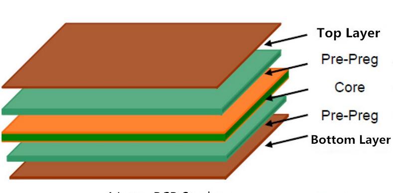
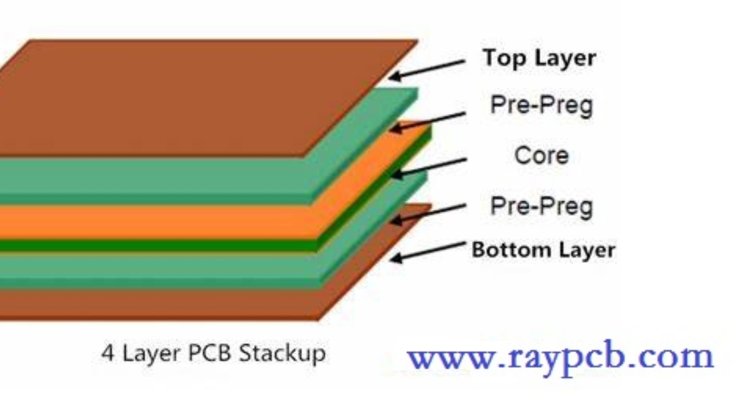
4 Layer Pcb - The Design Rules And How To Make A Rigid Pcb Stack Up
 www.hx-circuit.com
Complete Guide To PCB Layout Design Steps And Rules - Jhdpcb
 jhdpcb.com
PCB Layup Design Advantages Of Multilayer PCB
 www.01pcb.com
PCB Stackup Planning - Simple - Artist 3D
 artist-3d.com
PCB Layer Stack Up And Rules To Properly Design - Jarnistech
 www.jarnistech.com
Pcb layer stack up and rules to properly design. Pcb layout. Tips for pcb layout service